TOP221 Ver la hoja de datos (PDF) - Power Integrations, Inc
Número de pieza
componentes Descripción
Fabricante
TOP221 Datasheet PDF : 20 Pages
| |||
This product is not recommended for new designs.
TOP221-227
TOPSwitch-II Family
Three-Terminal Off-Line PWM Switch
Product Highlights
• Lowest cost, lowest component count switcher solution
• Cost competitive with linears above 5 W
• Very low AC/DC losses – up to 90% efficiency
• Built-in Auto-restart and Current limiting
• Latching Thermal shutdown for system level protection
• Implements Flyback, Forward, Boost or Buck topology
• Works with primary or opto feedback
• Stable in discontinuous or continuous conduction mode
• Source connected tab for low EMI
• Circuit simplicity and Design Tools reduce time to market
Description
The second generation TOPSwitch™-II family is more cost
effective and provides several enhancements over the first
generation TOPSwitch family. The TOPSwitch-II family
extends the power range from 100W to 150W for 100/115/
230 VAC input and from 50W to 90W for 85-265 VAC univer-
sal input. This brings TOPSwitch technology advantages
to many new applications, i.e. TV, Monitor, Audio amplifiers,
etc. Many significant circuit enhancements that reduce the
sensitivity to board layout and line transients now make the
design even easier. The standard 8L PDIP package option
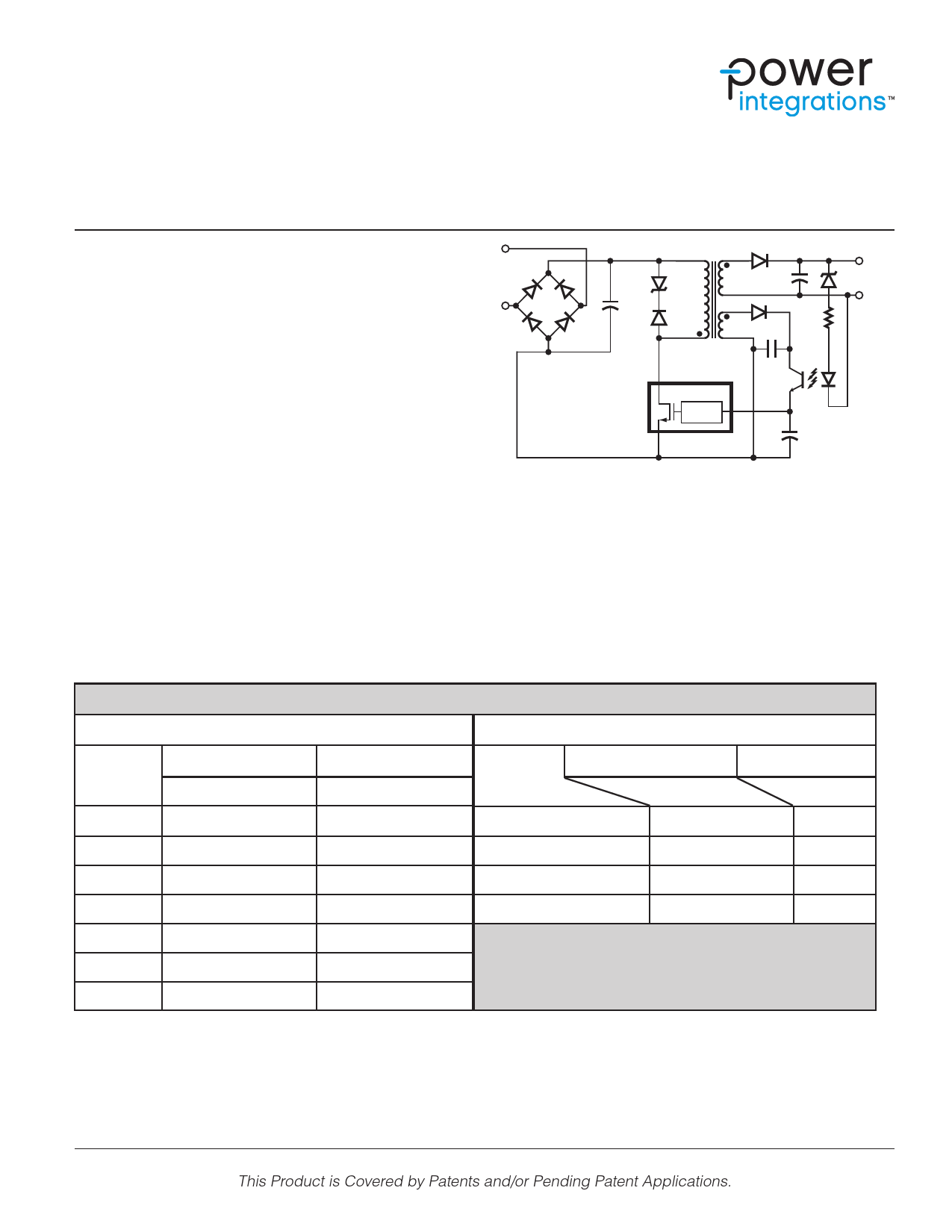
AC
IN
D
TOPSwitch
CONTROL
C
S
Figure 1. Typical Flyback Application.
PI-1951-091996
reduces cost in lower power, high efficiency applications.
The internal lead frame of this package uses six of its pins to
transfer heat from the chip directly to the board, eliminating
the cost of a heat sink. TOPSwitch incorporates all functions
necessary for a switched mode control system into a three
terminal monolithic IC: power MOSFET, PWM controller, high
voltage start up circuit, loop compensation and fault protec-
tion circuitry.
Output Power Table
TO-220 (Y) Package1
PART
ORDER
NUMBER
Single Voltage Input 3
100/115/230 VAC ±15%
P 4,6
MAX
Wide Range Input
85 to 265 VAC
P 4,6
MAX
TOP221YN
12 W
7W
TOP222YN
25 W
15 W
8L PDIP (P) or 8L SMD (G) Package2
PART
ORDER
NUMBER
Single Voltage Input3
100/115/230 VAC ±15%
P 5,6
MAX
Wide Range Input
85 to 265 VAC
P 5,6
MAX
TOP221PN or TOP221GN
9W
6W
TOP222PN or TOP222GN
15 W
10 W
TOP223YN
50 W
30 W
TOP223PN or TOP223GN
25 W
15 W
TOP224YN
75 W
45 W
TOP224PN or TOP224GN
30 W
20 W
TOP225YN
100 W
60 W
TOP226YN
125 W
75 W
TOP227YN
150 W
90 W
Notes: 1. Package outline: TO-220/3 2. Package Outline: DIP-8 or SMD-8 3. 100/115 VAC with doubler input 4. Assumes appro-
priate heat sinking to keep the maximum TOPSwitch junction temperature below 100 °C. 5. Soldered to 1 sq. in. (6.45 cm2), 2 oz.
copper clad (610 gm/m2) 6. PMAX is the maximum practical continuous power output level for conditions shown. The continuous
power capability in a given application depends on thermal environment, transformer design, efficiency required, minimum spec-
ified input voltage, input storage capacitance, etc. 7. Refer to key application considerations section when using TOPSwitch-II in
an existing TOPSwitch design.
www.power.com
This Product is Covered by Patents and/or Pending Patent Applications.
August 2016
Share Link: 