MCM69P735ZP2.5 Ver la hoja de datos (PDF) - Motorola => Freescale
Número de pieza
componentes Descripción
Fabricante
MCM69P735ZP2.5 Datasheet PDF : 16 Pages
| |||
DC OPERATING CONDITIONS AND CHARACTERISTICS
(3.6 V ≥ VDD ≥ 3.135 V, 70°C ≥ TA ≥ 0°C, Unless Otherwise Noted)
RECOMMENDED OPERATING CONDITIONS (Voltages Referenced to VSS = 0 V)
Parameter
Symbol
Min
Typ
Supply Voltage
I/O Supply Voltage
Ambient Temperature
Input Low Voltage
Input High Voltage
VDD
3.135
3.3
VDDQ
2.375
3.3
TA
0
—
VIL
– 0.3
—
VIH
2.0
—
VIH
Max
Unit
3.6
V
VDD
V
70
°C
0.8
V
VDD + 0.3
V
VSS
VSS – 1.0 V
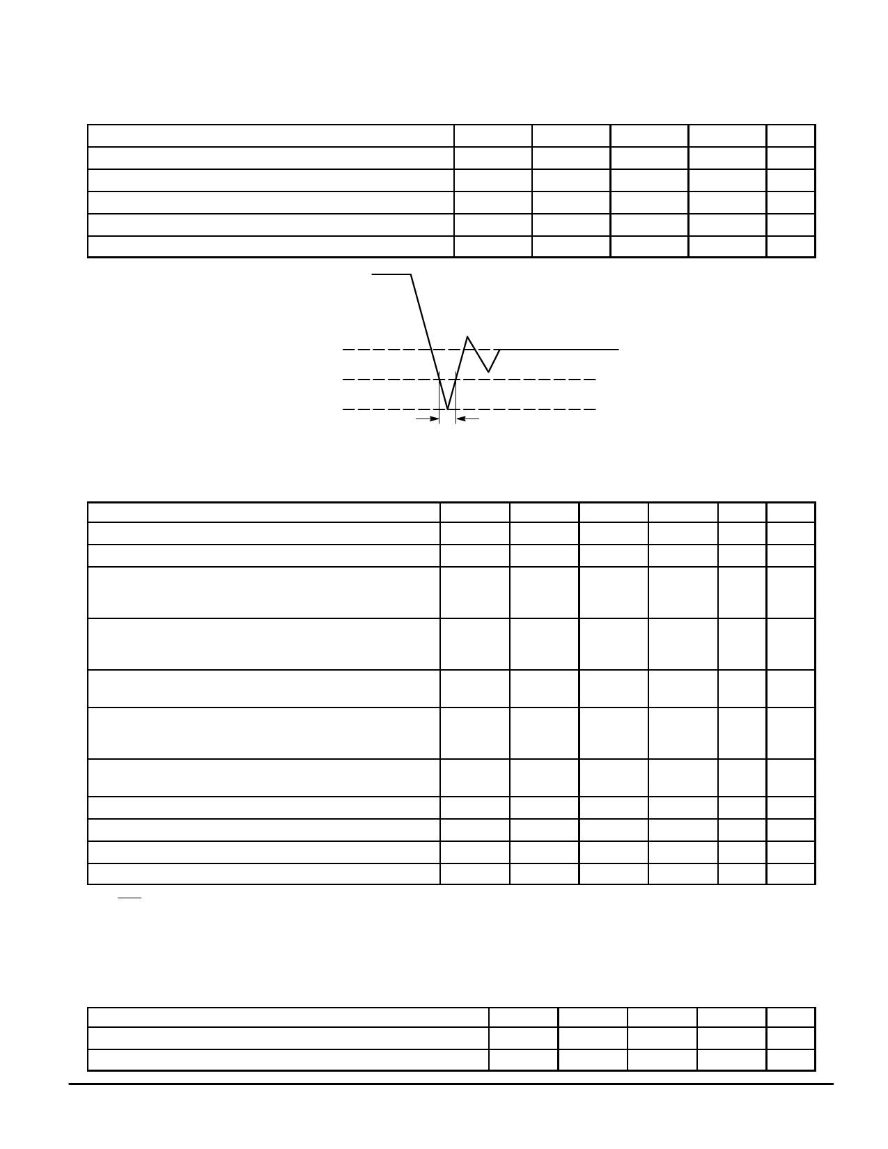
20% tKHKH (MIN)
Figure 1. Undershoot Voltage
DC CHARACTERISTICS AND SUPPLY CURRENTS
Parameter
Symbol
Min
Typ
Max
Input Leakage Current (0 V ≤ Vin ≤ VDD)
Ilkg(I)
—
Output Leakage Current (0 V ≤ Vin ≤ VDDQ)
Ilkg(O)
—
AC Supply Current (Device Selected,
All Outputs Open, Freq = Max)
Includes VDD and VDDQ
MCM69P735–2.5 IDDA
—
MCM69P735–3
MCM69P735–3.5
—
±1
—
±1
—
475
450
425
CMOS Standby Supply Current (Device Deselected, Freq = 0,
ISB2
—
—
40
VDD = Max, All Inputs Static at CMOS Levels Vin ≤ VSS + 0.2 V
or ≥ VDD – 0.2 V)
TTL Standby Supply Current (Device Deselected, Freq = 0,
VDD = Max, All Inputs Static at Vin ≤ VIL or ≥ VIH)
ISB3
—
—
45
Clock Running (Device Deselected,
MCM69P735–2.5 ISB4
—
Freq = Max, VDD = Max, All Inputs Toggling at
CMOS Levels Vin ≤ VSS + 0.2 V or ≥ VDD – 0.2 V)
—
190
Static Clock Running (Device Deselected,
MCM69P735–2.5 ISB5
—
—
85
Freq = Max, VDD = Max, All Inputs Static at Vin ≤ VIL or ≥ VIH)
Output Low Voltage (IOL = 2 mA) VDDQ = 2.5 V
VOL1
—
—
0.7
Output High Voltage (IOH = – 2 mA) VDDQ = 2.5 V
VOH1
1.7
—
—
Output Low Voltage (IOL = 8 mA) VDDQ = 3.3 V
VOL2
—
—
0.4
Output High Voltage (IOH = – 4 mA) VDDQ = 3.3 V
VOH2
2.4
—
—
NOTES:
1. LBO pin has an internal pullup and will exhibit leakage currents of ± 5 µA.
2. Reference AC Operating Conditions and Characteristics for input and timing (VIH/VIL, tr / tf, pulse level 0 to 3.0 V).
3. All addresses transition simultaneously low (LSB) and then high (MSB).
4. Data states are all zero.
5. Device in Deselected mode as defined by the Truth Table.
Unit Notes
µA
1
µA
mA 2, 3, 4
mA
5
mA
5
mA
5
mA
5
V
V
V
V
CAPACITANCE (f = 1.0 MHz, dV = 3.0 V, 70°C ≥ TA ≥ 0°C, Periodically Sampled Rather Than 100% Tested)
Parameter
Symbol
Min
Typ
Input Capacitance
Cin
—
4
Input/Output Capacitance
CI/O
—
7
Max
Unit
5
pF
8
pF
MOTOROLA FAST SRAM
MCM69P735
7
Share Link: 