MC100EP11DG Ver la hoja de datos (PDF) - ON Semiconductor
Número de pieza
componentes Descripción
Fabricante
MC100EP11DG Datasheet PDF : 11 Pages
| |||
MC10EP11, MC100EP11
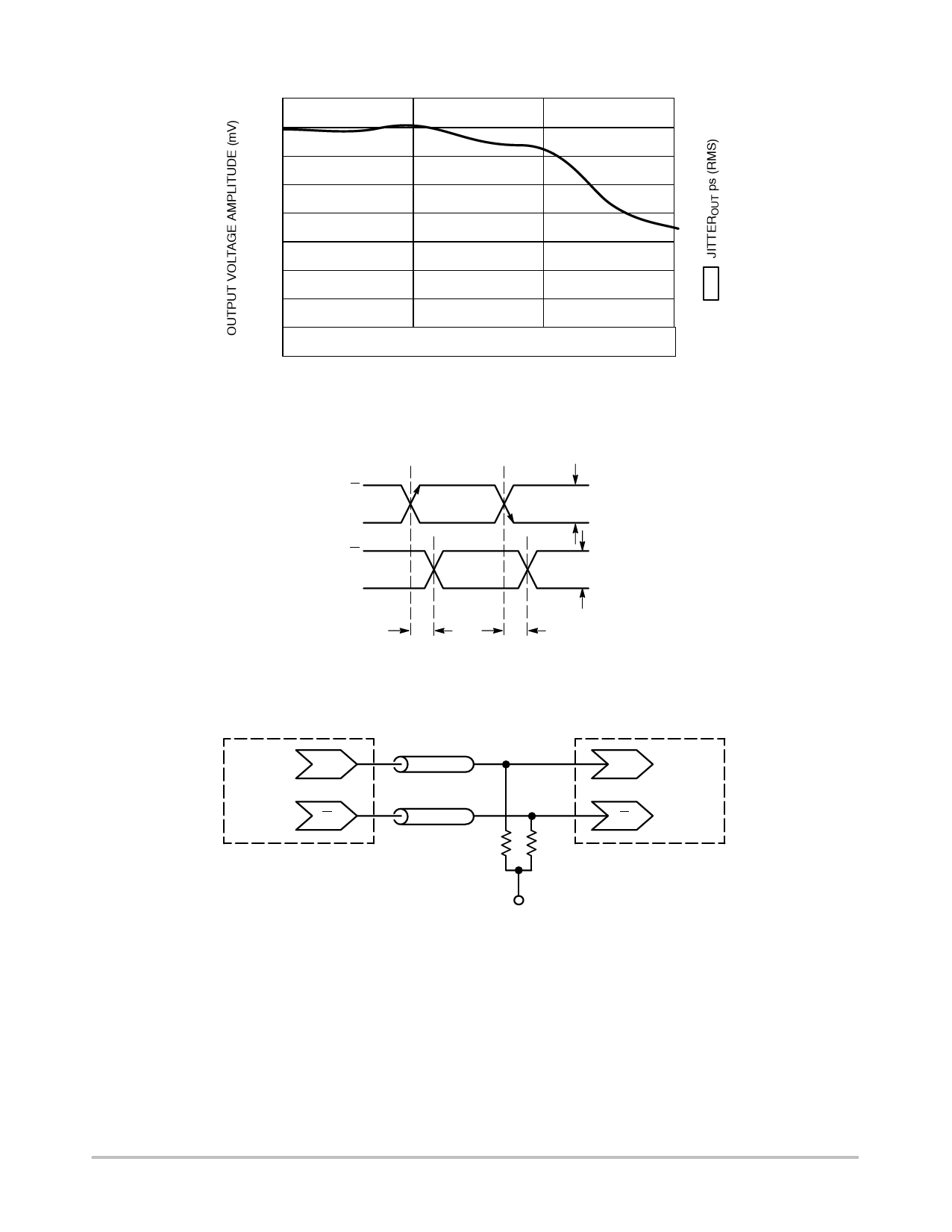
900
9
800
8
700
7
600
6
500
5
400
4
123000ÉÉ0000 ÉÉÉÉÉÉÉÉÉÉÉÉÉÉÉÉÉÉÉÉÉÉÉÉÉÉÉÉÉÉÉÉÉÉ123ÉÉÉÉ
0
1000
2000
3000
INPUT FREQUENCY (MHz)
Figure 2. Output Voltage Amplitude (VOUTPP) RMS Jitter vs. Input Clock Frequency at Ambient Temperature
D
VINPP = VIH(CLK) − VIL(CLK)
D
Q
VOUTPP = VOH(Q) − VOL(Q)
Q
tPLH
tPHL
Figure 3. AC Reference Measurement
Q
Driver
Device
Q
Zo = 50 W
Zo = 50 W
50 W
50 W
D
Receiver
Device
D
VTT
VTT = VCC − 2.0 V
Figure 4. Typical Termination for Output Driver and Device Evaluation
(See Application Note AND8020/D − Termination of ECL Logic Devices.)
http://onsemi.com
7
Share Link: 