MC100EP11DR2 Ver la hoja de datos (PDF) - ON Semiconductor
Número de pieza
componentes Descripción
Fabricante
MC100EP11DR2 Datasheet PDF : 11 Pages
| |||
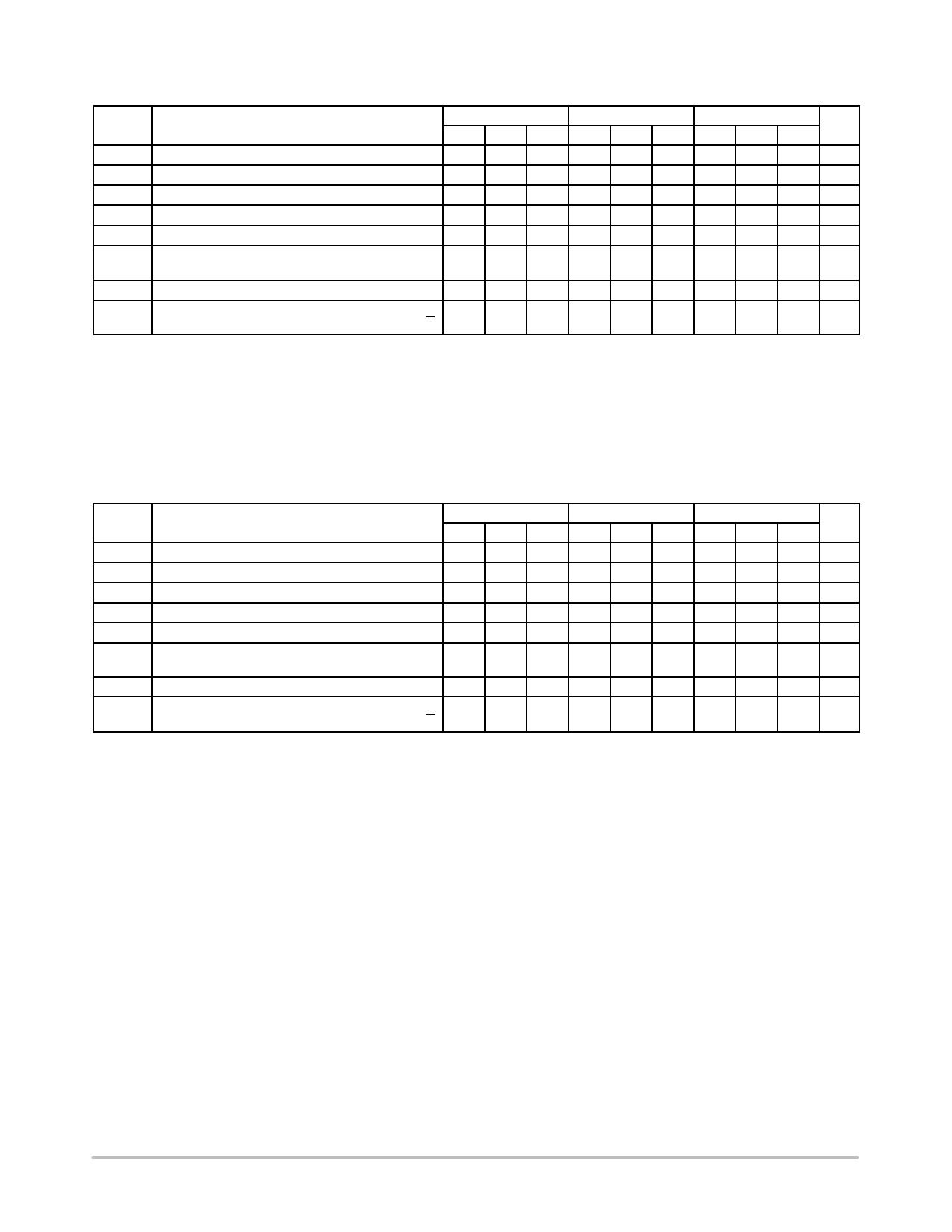
MC10EP11, MC100EP11
Table 7. 100EP DC CHARACTERISTICS, PECL VCC = 3.3 V, VEE = 0 V (Note 11)
−40°C
25°C
85°C
Symbol
IEE
VOH
VOL
VIH
VIL
VIHCMR
Characteristic
Negative Power Supply Current
Output HIGH Voltage (Note 12)
Output LOW Voltage (Note 12)
Input HIGH Voltage (Single−Ended)
Input LOW Voltage (Single−Ended)
Input HIGH Voltage Common Mode Range (Dif-
ferential Configuration) (Note 13)
Min Typ Max Min Typ Max Min Typ Max Unit
26 35 44 26 35 44 26 35 46 mA
2155 2280 2405 2155 2280 2405 2155 2280 2405 mV
1355 1480 1605 1355 1480 1605 1355 1480 1605 mV
2075
2420 2075
2420 2075
2420 mV
1355
1675 1355
1675 1355
1675 mV
2.0
3.3 2.0
3.3 2.0
3.3 V
IIH
Input HIGH Current
IIL
Input LOW Current
D 0.5
D −150
150
0.5
−150
150
0.5
−150
150 mA
mA
NOTE: Device will meet the specifications after thermal equilibrium has been established when mounted in a test socket or printed circuit
board with maintained transverse airflow greater than 500 lfpm. Electrical parameters are guaranteed only over the declared
operating temperature range. Functional operation of the device exceeding these conditions is not implied. Device specification limit
values are applied individually under normal operating conditions and not valid simultaneously.
11. Input and output parameters vary 1:1 with VCC. VEE can vary +0.3 V to −2.2 V.
12. All loading with 50 W to VCC − 2.0 V.
13. VIHCMR min varies 1:1 with VEE, VIHCMR max varies 1:1 with VCC. The VIHCMR range is referenced to the most positive side of the differential
input signal.
Table 8. 100EP DC CHARACTERISTICS, PECL VCC = 5.0 V, VEE = 0 V (Note 14)
−40°C
25°C
85°C
Symbol
IEE
VOH
VOL
VIH
VIL
VIHCMR
Characteristic
Negative Power Supply Current
Output HIGH Voltage (Note 15)
Output LOW Voltage (Note 15)
Input HIGH Voltage (Single−Ended)
Input LOW Voltage (Single−Ended)
Input HIGH Voltage Common Mode Range
(Differential Configuration) (Note 16)
Min Typ Max Min Typ Max Min Typ Max Unit
26 35 44 26 35 44 26 35 46 mA
3855 3980 4105 3855 3980 4105 3855 3980 4105 mV
3055 3180 3305 3055 3180 3305 3055 3180 3305 mV
3775
4120 3775
4120 3775
4120 mV
3055
3375 3055
3375 3055
3375 mV
2.0
5.0 2.0
5.0 2.0
5.0 V
IIH
Input HIGH Current
IIL
Input LOW Current
D 0.5
D −150
150
0.5
−150
150
0.5
−150
150 mA
mA
NOTE: Device will meet the specifications after thermal equilibrium has been established when mounted in a test socket or printed circuit
board with maintained transverse airflow greater than 500 lfpm. Electrical parameters are guaranteed only over the declared
operating temperature range. Functional operation of the device exceeding these conditions is not implied. Device specification limit
values are applied individually under normal operating conditions and not valid simultaneously.
14. Input and output parameters vary 1:1 with VCC. VEE can vary +2.0 V to −0.5 V.
15. All loading with 50 W to VCC − 2.0 V.
16. VIHCMR min varies 1:1 with VEE, VIHCMR max varies 1:1 with VCC. The VIHCMR range is referenced to the most positive side of the differential
input signal.
http://onsemi.com
5
Share Link: 