MC100EP11DG(2016) Ver la hoja de datos (PDF) - ON Semiconductor
Número de pieza
componentes Descripción
Fabricante
MC100EP11DG Datasheet PDF : 12 Pages
| |||
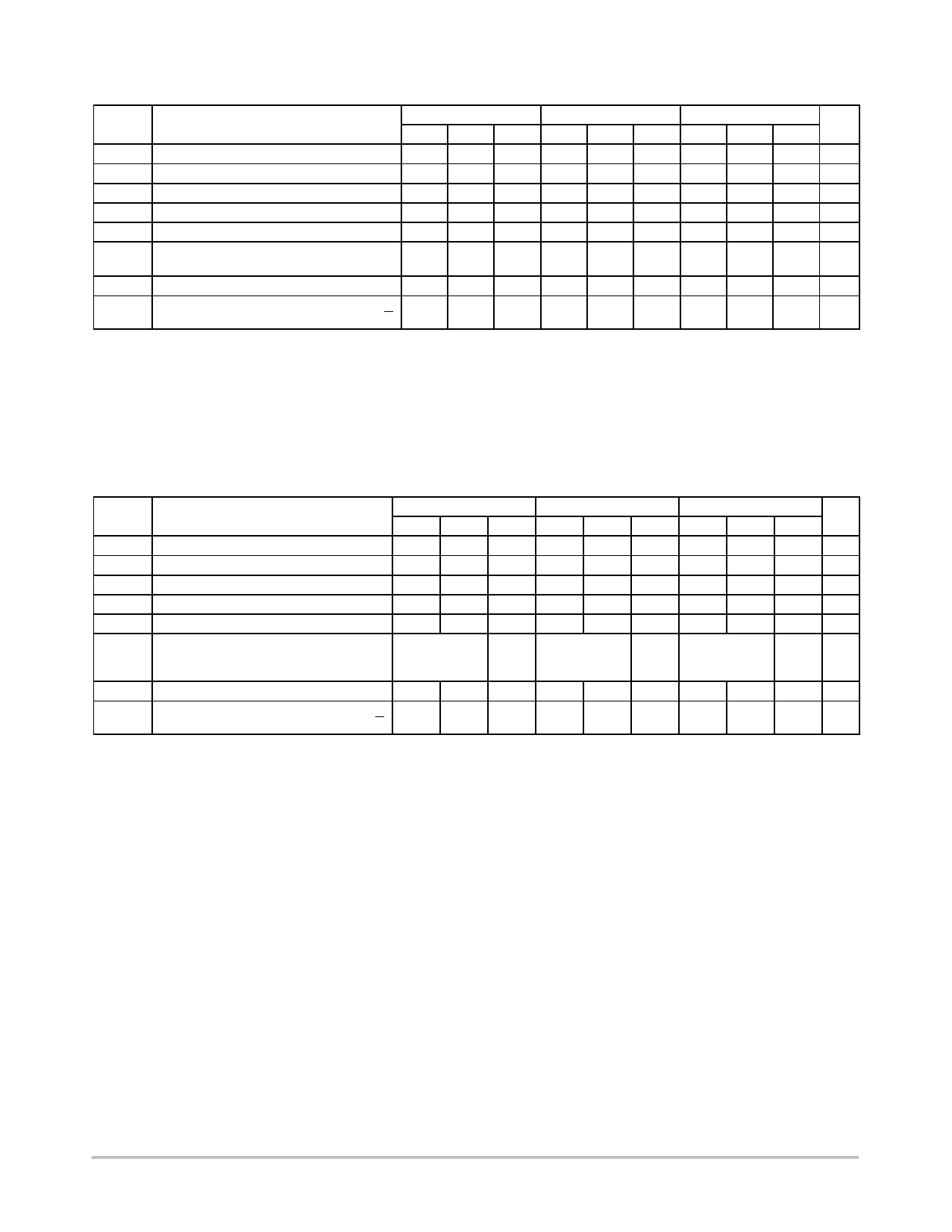
MC10EP11, MC100EP11
Table 5. 10EP DC CHARACTERISTICS, PECL (VCC = 5.0 V, VEE = 0 V (Note 1))
−40°C
25°C
85°C
Symbol
IEE
VOH
VOL
VIH
VIL
VIHCMR
Characteristic
Negative Power Supply Current
Output HIGH Voltage (Note 2)
Output LOW Voltage (Note 2)
Input HIGH Voltage (Single-Ended)
Input LOW Voltage (Single-Ended)
Input HIGH Voltage Common Mode
Range (Differential Configuration) (Note 3)
Min
20
3865
3065
3790
3065
2.0
Typ
29
3990
3190
Max
37
4115
3315
4115
3390
5.0
Min
20
3930
3130
3855
3130
2.0
Typ
30
4055
3255
Max
39
4180
3380
4180
3455
5.0
Min
22
3990
3190
3915
3190
2.0
Typ
31
4115
3315
Max Unit
40 mA
4240 mV
3440 mV
4240 mV
3515 mV
5.0 V
IIH
Input HIGH Current
IIL
Input LOW Current
D
D
0.5
−150
150
0.5
−150
150
0.5
−150
150 mA
mA
NOTE: Device will meet the specifications after thermal equilibrium has been established when mounted in a test socket or printed circuit
board with maintained transverse airflow greater than 500 lfpm. Electrical parameters are guaranteed only over the declared
operating temperature range. Functional operation of the device exceeding these conditions is not implied. Device specification limit
values are applied individually under normal operating conditions and not valid simultaneously.
1. Input and output parameters vary 1:1 with VCC.
2. All loading with 50 W to VCC − 2.0 V.
3. VIHCMR min varies 1:1 with VEE, VIHCMR max varies 1:1 with VCC. The VIHCMR range is referenced to the most positive side of the differential
input signal.
Table 6. 10EP DC CHARACTERISTICS, NECL (VCC = 0 V; VEE = −5.5 V to −3.0 V (Note 1))
−40°C
25°C
85°C
Symbol
Characteristic
Min Typ Max Min Typ Max Min Typ Max Unit
IEE
VOH
VOL
VIH
VIL
VIHCMR
Negative Power Supply Current
Output HIGH Voltage (Note 2)
Output LOW Voltage (Note 2)
Input HIGH Voltage (Single-Ended)
Input LOW Voltage (Single-Ended)
Input HIGH Voltage Common Mode
Range (Differential Configuration)
(Note 3)
20
29
37
20
30
39
22
31
40 mA
−1135 −1010 −885 −1070 −945 −820 −1010 −885 −760 mV
−1935 −1810 −1685 −1870 −1745 −1620 −1810 −1685 −1560 mV
−1210
−885 −1145
−820 −1085
−760 mV
−1935
−1610 −1870
−1545 −1810
−1485 mV
VEE + 2.0
0.0
VEE + 2.0
0.0
VEE + 2.0
0.0 V
IIH
Input HIGH Current
IIL
Input LOW Current
D
D
0.5
−150
150
0.5
−150
150
0.5
−150
150 mA
mA
NOTE: Device will meet the specifications after thermal equilibrium has been established when mounted in a test socket or printed circuit
board with maintained transverse airflow greater than 500 lfpm. Electrical parameters are guaranteed only over the declared
operating temperature range. Functional operation of the device exceeding these conditions is not implied. Device specification limit
values are applied individually under normal operating conditions and not valid simultaneously.
1. Input and output parameters vary 1:1 with VCC.
2. All loading with 50 W to VCC − 2.0 V.
3. VIHCMR min varies 1:1 with VEE, VIHCMR max varies 1:1 with VCC. The VIHCMR range is referenced to the most positive side of the differential
input signal.
www.onsemi.com
4
Share Link: 