GBJ2504 Ver la hoja de datos (PDF) - Chip Integration Technology Corporation
Número de pieza
componentes Descripción
Fabricante
GBJ2504
Chip Integration Technology Corporation

GBJ2504 Datasheet PDF : 3 Pages
| |||
GBJ25005 THRU GBJ2510
25A Miniature Glass Passivated Single-Phase Bridge Rectifiers
■ Features
• Surge overload ratings to 350 amperes peak.
• Recommended for non-automatic applications.
• Ideal for & save space on printed circuit board.
• Applicable for automatic insertion.
• Reliable low cost construction utilizing molded plastic
technology results in inexpensive product.
• Glass passivated chip junctions.
• Suffix "G" indicates Halogen-free part, ex.GBJ25005G.
• Lead-free parts meet RoHS requirments.
■ Mechanical data
• Epoxy:UL94-V0 rated flame retardant
• Case : Molded plastic, GBJ
• Terminals : Solder plated, solderable per
MIL-STD-750, Method 2026
• Polarity : marked on body
• Mounting Position : Any
• Weight : Approximated 7.00 gram
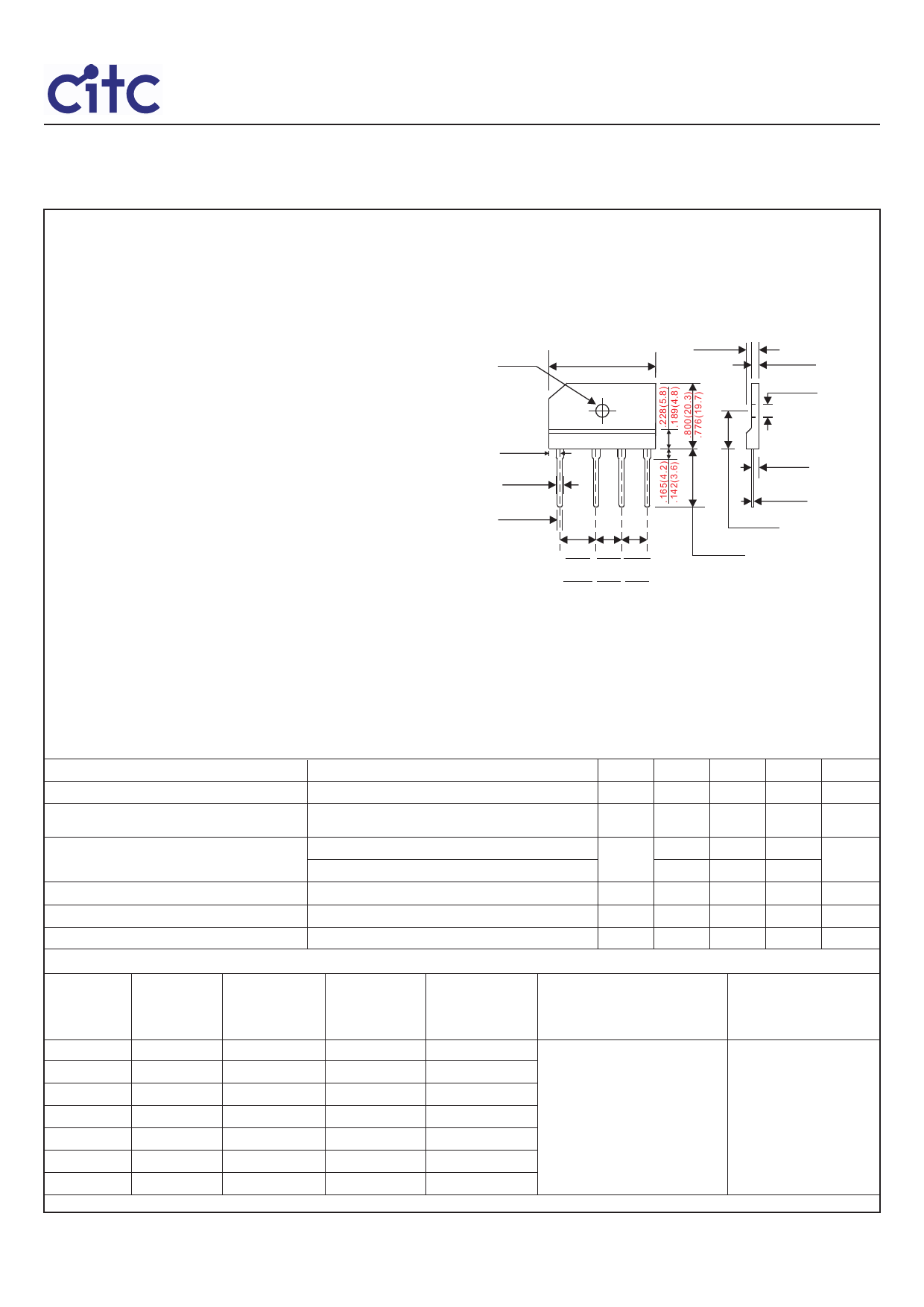
■ Outline
GBJ
hole for
#6 screw
1.193(30.3)
1.169(29.7)
+
.106(2.7)
.096(2.3)
.094(2.4)
.078(2.0)
.043(1.1)
.035(0.9)
~~–
.402 .303 .303
.386 .287 .287
(10.2) (7.7) (7.7)
(9.80) (7.3) (7.3)
.189(4.8)
.173(4.4)
.150(3.8)
.134(3.4)
.134(3.4)
.122(3.1)
Φ
.154(3.9)
.134(3.4)
.031(0.8)
.023(0.6)
.441(11.2)
.425(10.8)
.708(18.0)
.699(17.0)
Dimensions in inches and (millimeters)
■ Maximum ratings and electrical characteristics
Rating at 25OC ambient temperature unless otherwise specified. Single phase, half wave, 60Hz, resistive or inductive load.
For capacitive load, derate current by 20%.
Parameter
Forward rectified current
Forward surge current
Reverse current
Current squared time
Thermal resistance
Storage temperature
Conditions
with heatsink TC = 98OC
8.3ms single half sine-wave superimposed on
rate load (JEDEC method)
VR = VRRM TA = 25OC
VR = VRRM TA = 125OC
t < 8.3ms, TJ = 25OC
junction to ambient
Symbol
IO
IFSM
IR
I2t
RθJA
TSTG
MIN.
-55
TYP.
MAX.
25
350
10
500
508
22
+150
UNIT
A
A
uA
A2S
OC/W
OC
Symbol
GBJ25005
GBJ2501
GBJ2502
GBJ2504
GBJ2506
GBJ2508
GBJ2510
Max.
repetitive peak
Marking code
reverse voltage
VRRM (V)
GBJ25005
50
GBJ2501
100
GBJ2502
200
GBJ2504
400
GBJ2506
600
GBJ2508
800
GBJ2510
1000
Max.
RMS voltage
VRMS (V)
35
70
140
280
420
560
700
Max. DC
blocking voltage
VR (V)
50
100
200
400
600
800
1000
Max. forward voltage
@12.5A, TA = 25OC
VF (V)
1.1
Operating temperature
TJ (OC)
-55 ~ +150
Document ID : DS-21B07
1
Issued Date : 2010/05/05
Revised Date : 2012/05/31
Revision : C
Share Link: