KSZ9031RNX Ver la hoja de datos (PDF) - Microchip Technology
Número de pieza
componentes Descripción
Fabricante
KSZ9031RNX Datasheet PDF : 78 Pages
| |||
KSZ9031RNX
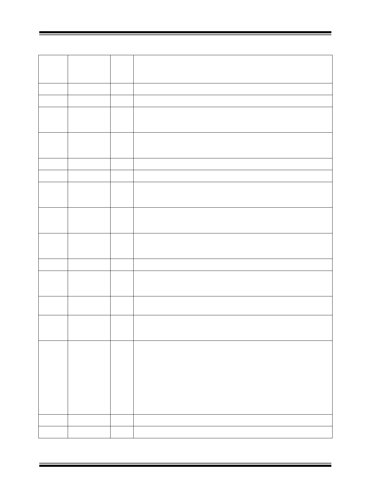
TABLE 2-1: SIGNALS - KSZ9031RNX (CONTINUED)
Pin
Number
25
26
27
28
29
30
31
32
33
34
35
36
37
38
39
40
Pin
Name
TX_EN
DVDDL
RXD3/
MODE3
RXD2/
MODE2
VSS
DVDDL
RXD1/
MODE1
RXD0/
MODE0
RX_DV/
CLK125_EN
DVDDH
RX_CLK/
PHYAD2
MDC
MDIO
INT_N/
PME_N2
DVDDL
DVDDH
Type
Note
2-1
Description
I
RGMII mode: RGMII TX_CTL (Transmit Control) input
P
1.2V digital VDD
RGMII mode: RGMII RD3 (Receive Data 3) output
I/O Config mode: The pull-up/pull-down value is latched as MODE3 during
power-up/reset. See the Strap-In Options - KSZ9031RNX section for details.
RGMII mode: RGMII RD2 (Receive Data 2) output
I/O Config mode: The pull-up/pull-down value is latched as MODE2 during
power-up/reset. See the Strap-In Options - KSZ9031RNX section for details.
GND Digital ground
P
1.2V digital VDD
RGMII mode: RGMII RD1 (Receive Data 1) output
I/O Config mode: The pull-up/pull-down value is latched as MODE1 during
power-up/reset. See the Strap-In Options - KSZ9031RNX section for details.
RGMII mode: RGMII RD0 (Receive Data 0) output
I/O Config mode: The pull-up/pull-down value is latched as MODE0 during
power-up/reset. See the Strap-In Options - KSZ9031RNX section for details.
RGMII mode: RGMII RX_CTL (Receive Control) output
I/O Config mode: Latched as CLK125_NDO Output Enable during power-up/
reset. See the Strap-In Options - KSZ9031RNX section for details.
P
3.3V, 2.5V, or 1.8V digital VDD_I/O
RGMII mode: RGMII RXC (Receive Reference Clock) output
I/O Config mode: The pull-up/pull-down value is latched as PHYAD[2] during
power-up/reset. See the Strap-In Options - KSZ9031RNX section for details.
Ipu
Management data clock input
This pin is the input reference clock for MDIO (Pin 37).
Ipu/O
O
Management data input/output
This pin is synchronous to MDC (Pin 36) and requires an external pull-up
resistor to DVDDH (digital VDD_I/O) in a range from 1.0 kΩ to 4.7 kΩ.
Interrupt output: Programmable interrupt output, with Register 1Bh as the
Interrupt Control/Status register, for programming the interrupt conditions and
reading the interrupt status. Register 1Fh, Bit [14] sets the interrupt output to
active low (default) or active high.
PME_N output: Programmable PME_N output (pin option 2). When asserted
low, this pin signals that a WOL event has occurred.
For Interrupt (when active low) and PME functions, this pin requires an exter-
nal pull-up resistor to DVDDH (digital VDD_I/O) in a range from 1.0 kΩ to
4.7 kΩ.
This pin is not an open-drain for all operating modes.
P
1.2V digital VDD
P
3.3V, 2.5V, or 1.8V digital VDD_I/O
DS00002117C-page 10
2016 Microchip Technology Inc.
Share Link: 