ICL7662 Ver la hoja de datos (PDF) - Renesas Electronics
Número de pieza
componentes Descripción
Fabricante
ICL7662 Datasheet PDF : 11 Pages
| |||
ICL7662
V+
10F
+
C1 -
1
8
2 ICL7662
7
3
6
4
5
10F
-
+
16A.
RO VOUT
-
VOUT = -V+
C2
V+
+
16B.
FIGURE 16. SIMPLE NEGATIVE CONVERTER AND ITS
OUTPUT EQUIVALENT
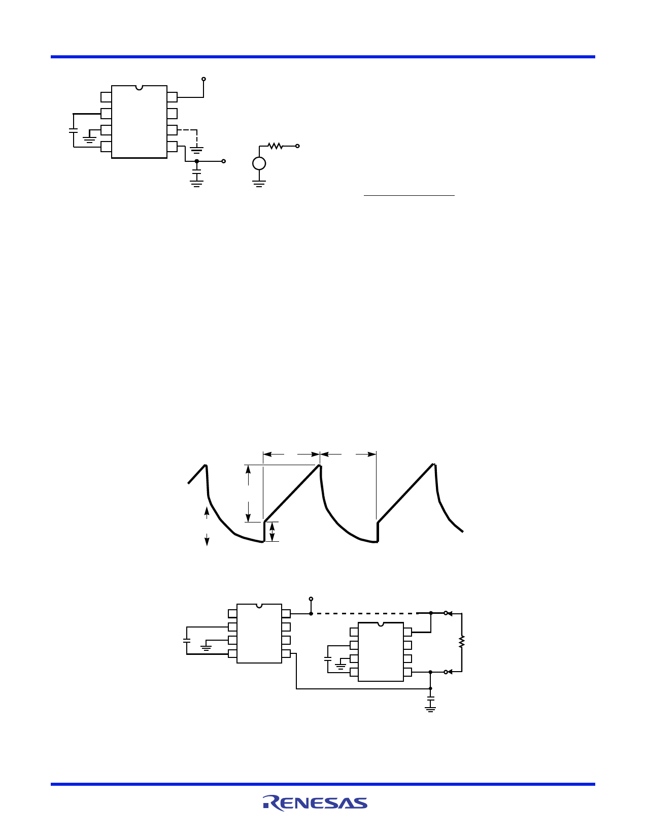
Output Ripple
ESR also affects the ripple voltage seen at the output. The total
ripple is determined by 2V, A and B, as shown in Figure 16.
Segment A is the voltage drop across the ESR of C2 at the
instant it goes from being charged by C1 (current flowing into
C2) to being discharged through the load (current flowing out of
C2). The magnitude of this current change is 2 x IOUT, hence
the total drop is 2 x IOUT x ESRC2V. Segment B is the voltage
change across C2 during time t2, the half of the cycle when C2
supplies current the load. The drop at B is IOUT x t2/C2V. The
peak-to-peak ripple voltage is the sum of these voltage drops:
VRIPPLE
-2---------f--P----U----1M-----P----------C----2--
+
2
ESRC2
IOU
T
Again, a low ESR capacitor will result in a higher performance
output.
Paralleling Devices
Any number of ICL7662 voltage converters may be paralleled
(Figure 18) to reduce output resistance. The reservoir
capacitor, C2, serves all devices while each device requires its
own pump capacitor, C1. The resultant output resistance would
be approximately:
ROUT =
ROUT (of ICL7662)
n (number of devices)
Cascading Devices
The ICL7662 may be cascaded as shown in Figure 19 to
produce larger negative multiplication of the initial supply
voltage. However, due to the finite efficiency of each device,
the practical limit is 10 devices for light loads. The output
voltage is defined by:
VOUT = -n(VIN),
where n is an integer representing the number of devices
cascaded. The resulting output resistance would be
approximately the weighted sum of the individual ICL7662 ROUT
values.
t2
t1
0
V
- (V+)
B
A
FIGURE 17. OUTPUT RIPPLE
V+
1
8
2 ICL7662 7
1
8
C1
3
“1”
6
4
5
C1
2 ICL7662 7
3
“N”
6
RL
4
5
-
+
C2
FIGURE 18. PARALLELING DEVICES
FN3181 Rev.4.00
Jan 9, 2006
Page 8 of 11
Share Link: 