PN2907A Ver la hoja de datos (PDF) - NXP Semiconductors.
Número de pieza
componentes Descripción
Fabricante
PN2907A Datasheet PDF : 7 Pages
| |||
NXP Semiconductors
PNP switching transistor
SYMBOL
PARAMETER
CONDITIONS
Switching times (between 10 % and 90 % levels); see Fig.2
ton
turn-on time
td
delay time
tr
rise time
toff
turn-off time
ts
storage time
tf
fall time
ICon = −150 mA; IBon = −15 mA;
IBoff = 15 mA
Product data sheet
PN2907A
MIN. MAX. UNIT
−
40
ns
−
12
ns
−
30
ns
−
365
ns
−
300
ns
−
65
ns
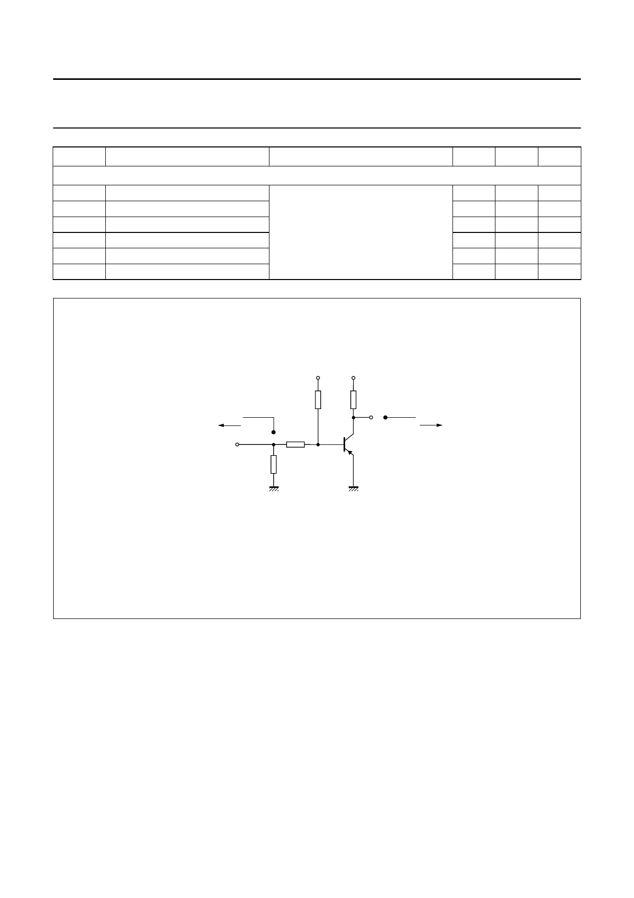
handbook, full pagewidth
VBB
VCC
(probe)
oscilloscope
450 Ω
Vi
RB
R2
R1
RC
Vo
(probe)
oscilloscope
450 Ω
DUT
MGD624
Vi = −9.5 V; T = 500 µs; tp = 10 µs; tr = tf ≤ 3 ns.
R1 = 68 Ω; R2 = 325 Ω; RB = 325 Ω; RC = 160 Ω.
VBB = 3.5 V; VCC = −29.5 V.
Oscilloscope: input impedance Zi = 50 Ω.
Fig.2 Test circuit for switching times.
2004 Oct 11
4
Share Link: 