X5328PI-2.7A Ver la hoja de datos (PDF) - Renesas Electronics
Número de pieza
componentes Descripción
Fabricante
X5328PI-2.7A Datasheet PDF : 21 Pages
| |||
X5328, X5329 (Replaces X25328, X25329)
The Write Enable Latch (WEL) bit indicates the Status of
the Write Enable Latch. When WEL = 1, the latch is set
HIGH and when WEL = 0 the latch is reset LOW. The
WEL bit is a volatile, read only bit. It can be set by the
WREN instruction and can be reset by the WRDS
instruction.
The block lock bits, BL0 and BL1, set the level of block
lock protection. These nonvolatile bits are programmed
using the WRSR instruction and allow the user to protect
one quarter, one half, all or none of the EEPROM array.
Any portion of the array that is block lock protected can
be read but not written. It will remain protected until the
BL bits are altered to disable block lock protection of that
portion of memory.
Status Register Bits Array Addresses Protected
BL1
BL0
X5328/X5329
0
0
None
0
1
$0C00-$0FFF
1
0
$0800-$0FFF
1
1
$0000-$0FFF
The FLAG bit shows the status of a volatile latch that can
be set and reset by the system using the SFLB and RFLB
instructions. The Flag bit is automatically reset upon
power-up.
The nonvolatile WPEN bit is programmed using the
WRSR instruction. This bit works in conjunction with the
WP pin to provide an In-Circuit Programmable ROM func-
tion (Table 2). WP is LOW and WPEN bit programmed
HIGH disables all Status Register Write Operations.
In Circuit Programmable ROM Mode
This mechanism protects the block lock and Watchdog
bits from inadvertent corruption.
In the locked state (Programmable ROM Mode) the WP pin
is LOW and the nonvolatile bit WPEN is “1”. This mode
disables nonvolatile writes to the device’s Status Register.
Setting the WP pin LOW while WPEN is a “1” while an
internal write cycle to the Status Register is in progress
will not stop this write operation, but the operation dis-
ables subsequent write attempts to the Status Register.
When WP is HIGH, all functions, including nonvolatile
writes to the Status Register operate normally.
Setting the WPEN bit in the Status Register to “0” blocks
the WP pin function, allowing writes to the Status Register
when WP is HIGH or LOW. Setting the WPEN bit to “1”
while the WP pin is LOW activates the Programmable
ROM mode, thus requiring a change in the WP pin prior to
subsequent Status Register changes. This allows manu-
facturing to install the device in a system with WP pin
grounded and still be able to program the Status Register.
Manufacturing can then load Configuration data, manu-
facturing time and other parameters into the EEPROM,
then set the portion of memory to be protected by setting
the block lock bits, and finally set the “OTP mode” by set-
ting the WPEN bit. Data changes now require a hardware
change.
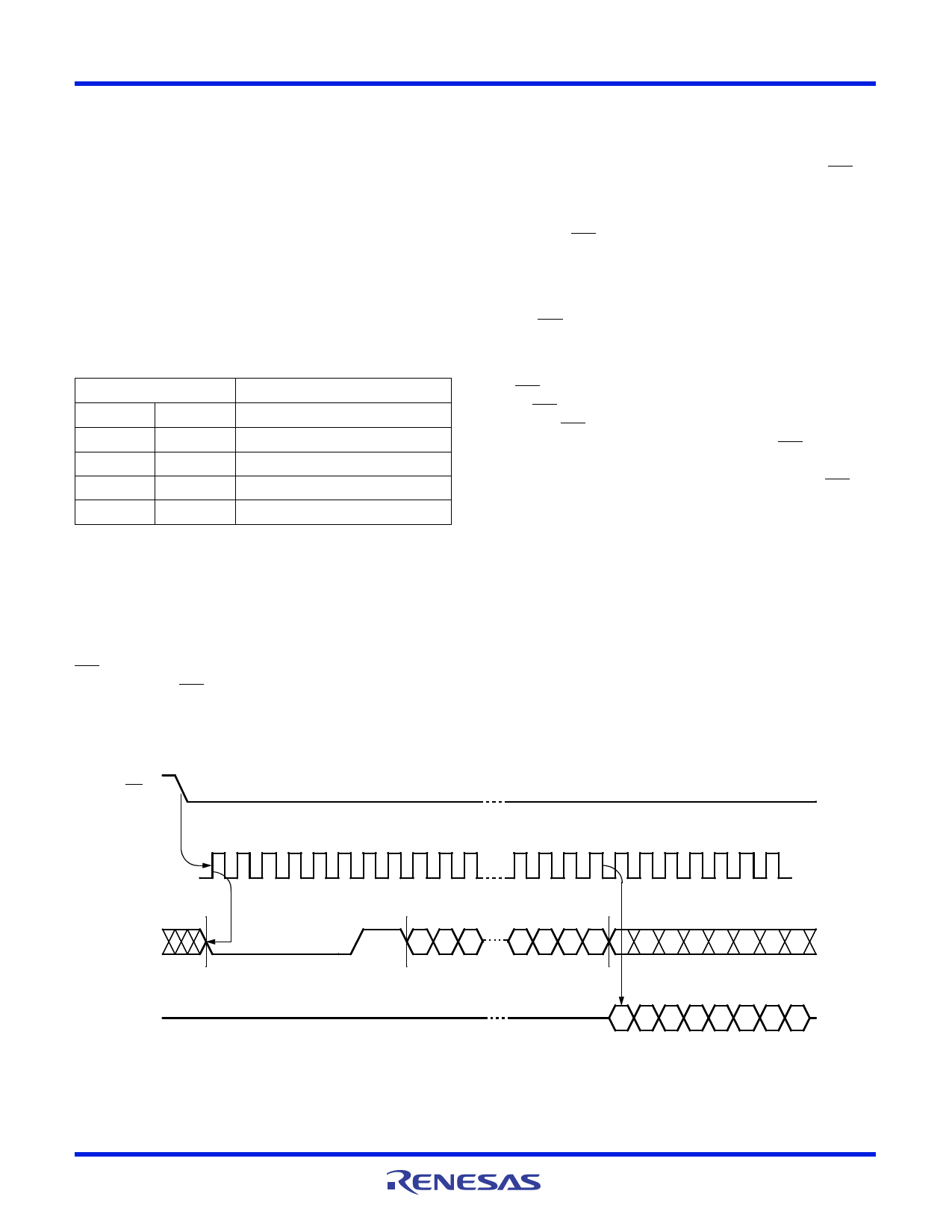
Figure 5. Read EEPROM Array Sequence
CS
SCK
0 1 2 3 4 5 6 7 8 9 10
20 21 22 23 24 25 26 27 28 29 30
Instruction
SI
16 Bit Address
15 14 13
3210
High Impedance
SO
Data Out
7 654321 0
MSB
FN8132 Rev 2.00
October 16, 2015
Page 7 of 21
Share Link: 