CXA1946AQ Ver la hoja de datos (PDF) - Sony Semiconductor
Número de pieza
componentes Descripción
Fabricante
CXA1946AQ Datasheet PDF : 24 Pages
| |||
CXA1946AQ/AR
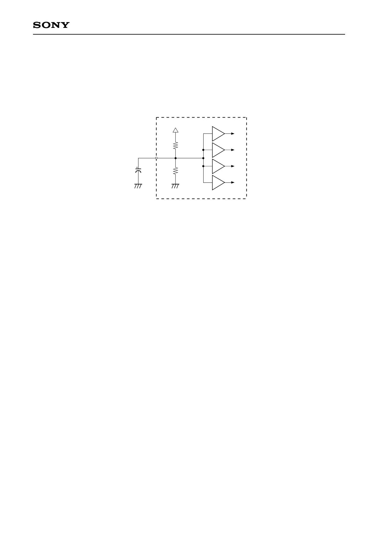
6. VCT buffer
The internal circuit for the VCT pin is shown in Fig. 8.
This circuit generates the electric potential for the center between Vcc and GND (Vcc/2). The IC internal
operation reference potential is equal to the output potential of VCT buffer. The impedance for the VCT pin
(Pin 17) is high since it is connected to a bypass capacitor. Add an external buffer when using the electric
potential of the VCT pin as the external reference potential for the CXA1946.
VCT
10µ
VCC
100k
100k
Fig. 8. VCT Buffer
7. Serial data I/O
The serial data has a 32-bit structure as indicated in the specifications. Data input is conducted using three
inputs: DATA, CLK, and CE. DATA is shifted in the CXA1946A internal shift register at the rising edge of
CLK. The data in the shift register is latched at the falling edge of CE. Refer to this specification for details
on the timing.
The CXA1946A does not have a reset (initialize) pin. The internal shift register and latch are reset
automatically when power is first supplied to the IC. To execute a reset at other times, send the data
(statuses after reset ) shown in the item "RESET" of this specification to the CXA1946A.
8. Zero-cross detector (with timer)
Using the zero-cross detector, the internal latch data is overwritten the first time the input signal becomes
roughly 0 after serial data is sent (after CE goes low). This operation reduces noise when overwriting data.
Although there are usually no problems when a normal audio signal is input, in rare cases there may be
nothing except a large-amplitude input signal of the high band, causing the slew rate to become abnormally
high; the zero-cross detection signal is not output in such a case because the zero-cross detector response
speed is too slow. Another rare situation would be that the zero-cross detection signal is output very
infrequently because the input signal frequency is extremely low. In these types of instances, it is
conceivable that the internal latch data will not be overwritten after data is sent, or that it will take much time
until the data is overwritten. Therefore, to an external observer it will appear that the data is not being
overwritten regardless of the fact that data is being sent.
As a countermeasure, the IC is designed to permit the internal latch data to be forcibly overwritten if the
zero-cross detection signal is not output within a certain waiting period after the data is sent (after CE goes
low). This function is called the “timer.” If the zero-cross detection signal is output within a certain waiting
period, the internal latch data is overwritten in synchronization with the zero-cross of the input signal.
The waiting period mentioned above can be changed according to the value of the external capacitor
connected to the TIMER pin. When the value of the capacitor is 0.01µF, the waiting period is approximately
500µs.
9. Power-off mute
When Vcc goes below 5V, the output stage bias of the fader output pins FNTO1, FNTO2, REO1, and
REO2 is turned off and the pins go to high impedance. This operation prevents popping noises caused by
the output pin potential deviating from Vcc/2 when the power is turned off.
– 21 –
Share Link: 