TOP209 Ver la hoja de datos (PDF) - Power Integrations, Inc
Número de pieza
componentes Descripción
Fabricante
TOP209 Datasheet PDF : 16 Pages
| |||
TOP209/210
1
T1
T1RD2
BR1
+ DFO6M
RA
470 kΩ
-
JP1*
JUMPER
C1
10 µF
200 V
VR1
BZY97-C200
D1
UF4005
2
D2
MBR360
8
L1
3 µH
12 V
RB
470 kΩ
C9
10 µF
200 V
D TOPSwitch
R1
CONTROL
C
6.8 Ω
3
L2
12 mH min.
0.2A
S
U1
TOP210
D3
1N4148
C5
47 µF
10 V
C6
47nF
250VAC
4
F1
X2
2A
C2
330 µF
16 V
5
C3
120 µF
16 V
R2
330
1W
RTN
CIRCUIT PERFORMANCE:
Line Regulation - –1%
(85-132 VAC) or
(170-265 VAC)
Load Regulation - –5%
(10-100%)
Ripple Voltage – 50 mV
Meets CISPR-22 Class B
L
C7
1nF
250 VAC
N
Y1
J1
* JPI INSTALLED FOR 110 VAC INPUT
JPI OPEN FOR 220 VAC INPUT
PI-2046-052397
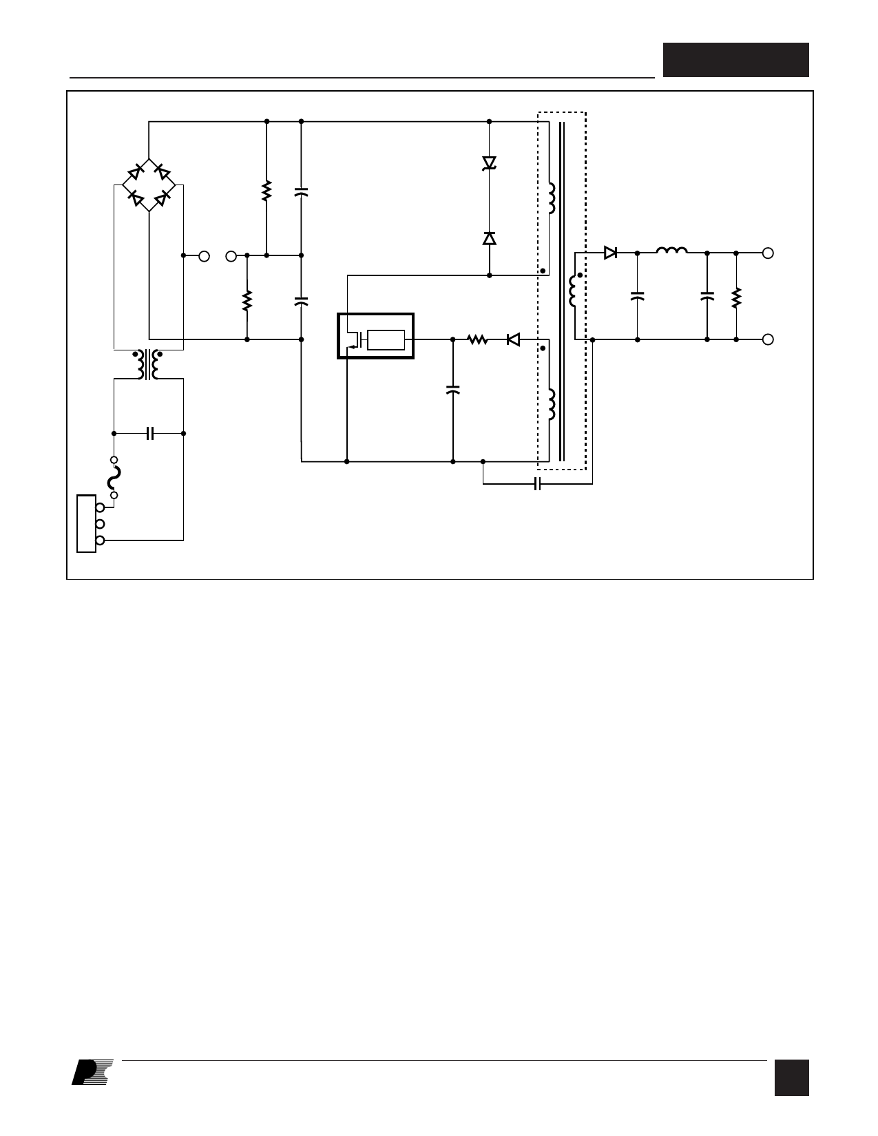
Figure 8. Schematic Diagram of a 12 V, 8 W 110/220 VAC Input Power Supply Using the TOP210.
The circuit shown in Figure 8 produces a 12 V, 8 W power
supply that operates from 85 to 132 VAC or 170 to 264 VAC
input voltage. The 12 V output voltage is determined by the
TOPSwitch CONTROL pin shunt regulator voltage, the voltage
drops of D2 and D3, and the turns ratio between the bias and
output windings of T1. Other output voltages are also possible
by adjusting the transformer turns ratios. R1 and C5 provide
filtering of the bias winding to improve line and load regulation.
AC power is rectified and filtered by BR1, C1 and C9 to create
the high voltage DC bus applied to the primary winding of T1.
The other side of the transformer primary is driven by the
integrated high-voltage MOSFET within the TOP210. JP1 is a
jumper used to select 110 VAC or 220 VAC operation. Installing
JP1 selects 110 VAC operation. Leaving JP1 open selects
220 VAC operation. RA and RB, which equalize voltage across
C1 and C9, are necessary only when JP1 is not installed. D1 and
VR1 clamp the leading-edge voltage spike caused by transformer
leakage inductance to a safe value and reduce ringing. The
power secondary winding is rectified and filtered by D2, C2,
L1, and C3 to create the 12 V output voltage. R2 provides a pre-
load on the 12 V output to improve load regulation at light loads.
The bias winding is rectified and filtered by D3, R1, and C5 to
create a bias voltage to the TOP210. L2 and Y1-capacitor C7
attenuate common-mode emission currents caused by high-
voltage switching waveforms on the DRAIN side of the primary
winding and the primary to secondary capacitance. L2 and C6
attenuate differential-mode emission currents caused by the
fundamental and harmonics of the trapezoidal primary current
waveform. C5 filters internal MOSFET gate drive charge
current spikes on the CONTROL pin, determines the auto-
restart frequency, and together with R1, compensates the control
loop.
7 A
8/97
Share Link: 