TOP210 Ver la hoja de datos (PDF) - Power Integrations, Inc
Número de pieza
componentes Descripción
Fabricante
TOP210 Datasheet PDF : 16 Pages
| |||
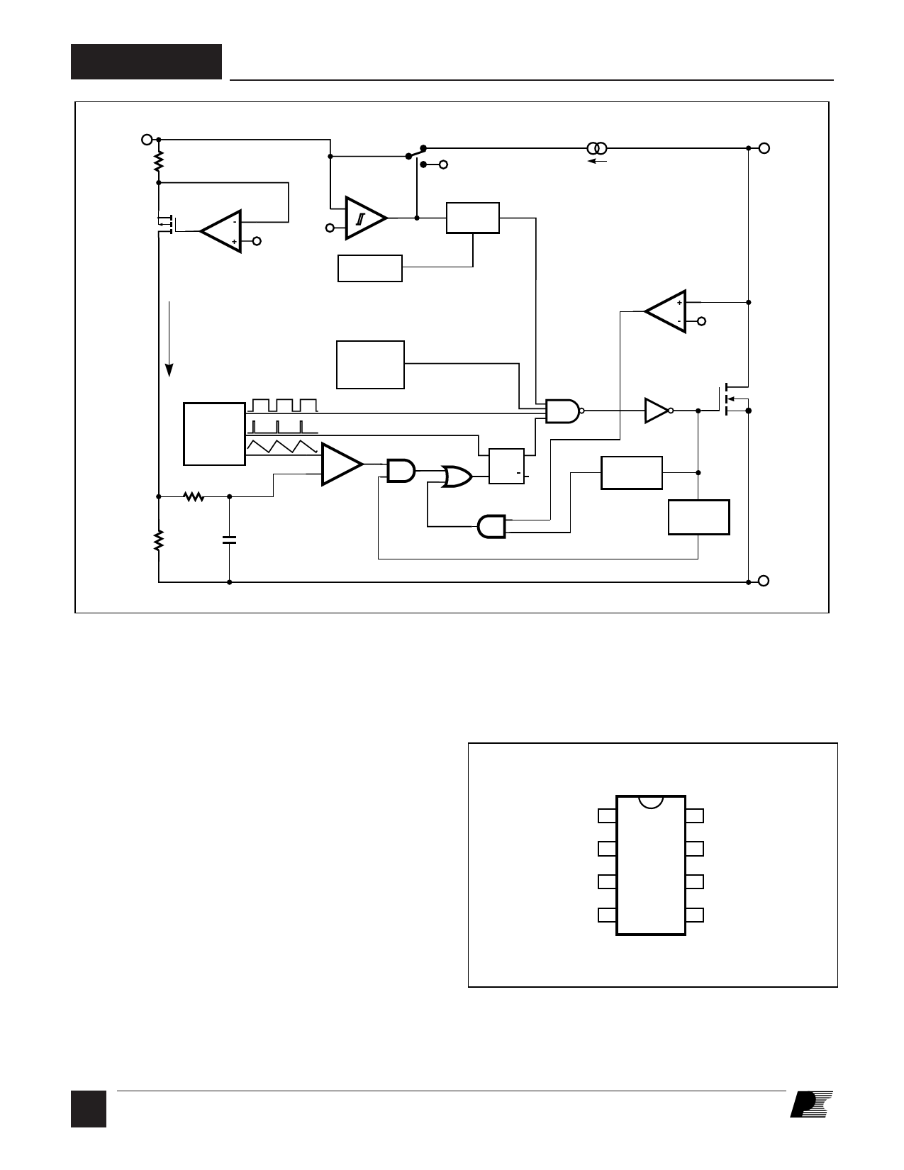
TOP209/210
CONTROL
VC
0
ZC
SHUNT REGULATOR/
ERROR AMPLIFIER
5.7 V
5.7 V
4.7 V
1
SHUTDOWN/
AUTO-RESTART
+
-
POWER-UP
RESET
INTERNAL
SUPPLY
÷8
IFB
OSCILLATOR
DMAX
CLOCK
SAW
RE
THERMAL
SHUTDOWN
WITH
HYSTERESIS
-
+
PWM
COMPARATOR
S
Q
R
Q
Figure 2. Functional Block Diagram.
DRAIN
VILIMIT
CONTROLLED
TURN-ON
GATE
DRIVER
LEADING
EDGE
BLANKING
MINIMUM
ON-TIME
DELAY
SOURCE
PI-1742-011796
Pin Functional Description
2 DRAIN Pin:
Output MOSFET drain connection. Provides internal bias
current during start-up operation via an internal switched high-
voltage current source. Internal current sense point.
CONTROL Pin:
Error amplifier and feedback current input pin for duty cycle
control. Internal shunt regulator connection to provide internal
bias current during normal operation. It is also used as the
supply bypass and auto-restart/compensation capacitor
connection point.
SOURCE Pin:
Control circuit common, internally connected to output
MOSFET source.
SOURCE (HV RTN) Pin:
Output MOSFET source connection for high voltage return.
SOURCE 1
8 SOURCE (HV RTN)
N/C 2
N/C 3
7 N/C
6 N/C
CONTROL 4
5 DRAIN
P Package (DIP-8)
G Package (SMD-8)
Figure 3. Pin Configuration.
PI—2044-040901
2A
8/97
Share Link: 