MC74HC4020A_11 Ver la hoja de datos (PDF) - ON Semiconductor
Número de pieza
componentes Descripción
Fabricante
MC74HC4020A_11 Datasheet PDF : 13 Pages
| |||
MC74HC4020A
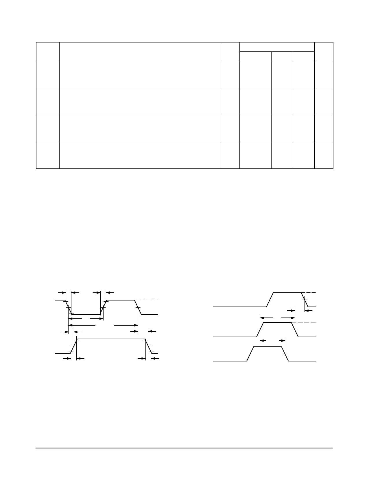
TIMING REQUIREMENTS (Input tr = tf = 6 ns)
Symbol
Parameter
trec Minimum Recovery Time, Reset Inactive to Clock
(Figure 2)
tw
Minimum Pulse Width, Clock
(Figure 1)
tw
Minimum Pulse Width, Reset
(Figure 2)
tr, tf Maximum Input Rise and Fall Times
(Figure 1)
Guaranteed Limit
VCC
V −55 to 25°C ≤85°C ≤125°C Unit
2.0
30
3.0
20
4.5
5
6.0
4
40
50
ns
25
30
8
12
6
9
2.0
70
3.0
40
4.5
15
6.0
13
80
90
ns
45
50
19
24
16
20
2.0
70
3.0
40
4.5
15
6.0
13
80
90
ns
45
50
19
24
16
20
2.0
1000
1000 1000 ns
3.0
800
800
800
4.5
500
500
500
6.0
400
400
400
PIN DESCRIPTIONS
INPUTS
Clock (Pin 10)
Negative−edge triggering clock input. A high−to−low
transition on this input advances the state of the counter.
Reset (Pin 11)
Active−high reset. A high level applied to this input
asynchronously resets the counter to its zero state, thus
forcing all Q outputs low.
OUTPUTS
Q1, Q4—Q14 (Pins 9, 7, 5, 4, 6, 13, 12, 14, 15, 1, 2, 3)
Active−high outputs. Each Qn output divides the Clock
input frequency by 2N.
SWITCHING WAVEFORMS
tf
tr
90%
VCC
Clock
50%
10%
GND
tw
1/fMAX
tPLH
tPHL
90%
Q1 50%
10%
tTLH
tTHL
Clock
Reset
Any Q
VCC
50%
GND
trec
tw
VCC
50%
GND
tPHL
50%
Figure 3.
Figure 4.
http://onsemi.com
6
Share Link: 