NX3V1T66_08 Ver la hoja de datos (PDF) - NXP Semiconductors.
Número de pieza
componentes Descripción
Fabricante
NX3V1T66_08 Datasheet PDF : 18 Pages
| |||
NXP Semiconductors
NX3V1T66
Low-voltage analog switch
Table 7. Static characteristics …continued
At recommended operating conditions; voltages are referenced to GND (ground 0 V).
Symbol Parameter Conditions
Tamb = 25 °C
Min Typ Max
CI
CS(OFF)
CS(ON)
input
capacitance
OFF-state
capacitance
ON-state
capacitance
- 1.0 -
- 70 -
- 205 -
Tamb = −40 °C to +125 °C Unit
Min Max Max
(85 °C) (125 °C)
-
-
- pF
-
-
- pF
-
-
- pF
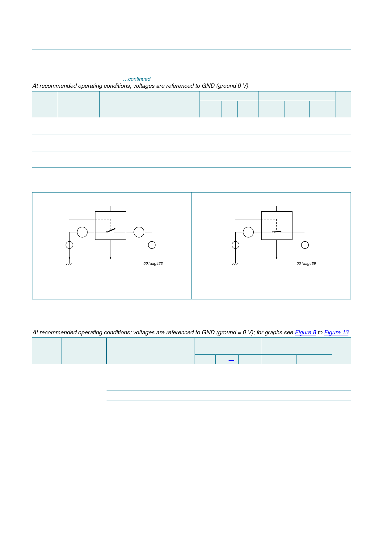
11.1 Test circuits
VCC
VIL
E
IS Z
VI
Y IS
GND
VO
VCC
VIH
E
IS Z
VI
Y
GND
VO
001aag488
Fig 5.
VI = 0.3 V or VCC − 0.3 V; VO = VCC − 0.3 V or 0.3 V.
Test circuit for measuring OFF-state leakage
current
001aag489
Fig 6.
VI = 0.3 V or VCC − 0.3 V; VO = open circuit.
Test circuit for measuring ON-state leakage
current
11.2 ON resistance
Table 8. Resistance RON
At recommended operating conditions; voltages are referenced to GND (ground = 0 V); for graphs see Figure 8 to Figure 13.
Symbol Parameter
Conditions
Tamb = −40 °C to +85 Tamb = −40 °C to +125 °C Unit
°C
Min Typ[1] Max
Min
Max
RON(peak) ON resistance
(peak)
VI = GND to VCC;
ISW = 100 mA; see Figure 7
VCC = 1.4 V
VCC = 1.65 V
VCC = 2.3 V
VCC = 2.7 V
-
0.8 1.9
-
-
0.5 0.8
-
-
0.3 0.5
-
-
0.25 0.45
-
2.1
Ω
0.9
Ω
0.6
Ω
0.5
Ω
NX3V1T66_2
Product data sheet
Rev. 02 — 24 July 2008
© NXP B.V. 2008. All rights reserved.
5 of 18
Share Link: 