MJ13333 Ver la hoja de datos (PDF) - ON Semiconductor
Número de pieza
componentes Descripción
Fabricante
MJ13333 Datasheet PDF : 8 Pages
| |||
ON Semiconductort
SWITCHMODEt Series
NPN Silicon Power Transistor
MJ13333
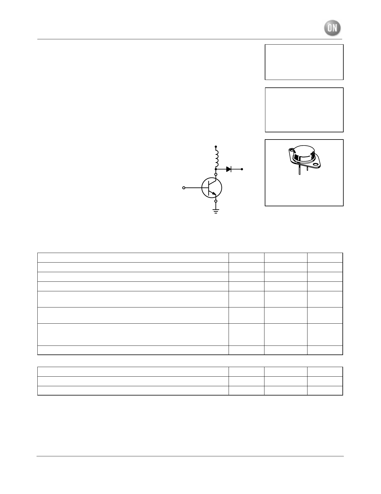
The MJ13333 transistor is designed for high voltage, high–speed,
power switching in inductive circuits where fall time is critical. It is
particularly suited for line operated SWITCHMODE applications
such as:
20 AMPERE
NPN SILICON
POWER TRANSISTORS
400–500 VOLTS
• Switching Regulators
175 WATTS
• Inverters
• Solenoid and Relay Drivers
• Motor Controls
• Deflection Circuits
• Fast Turn Off Times
200 ns Inductive Fall Time — 25_C (Typ)
1.8 µs Inductive Storage Time — 25_C (Typ)
• Operating Temperature Range –65 to +200_C
CASE 1–07
TO–204AA
(TO–3)
• 100_C Performance Specified for:
Reversed Biased SOA with Inductive Loads
Switching Times with Inductive Loads
Saturation Voltages
Leakage Currents
ÎÎÎÎÎÎÎÎÎÎÎÎÎÎÎÎÎÎÎÎÎÎÎÎÎÎÎÎÎÎÎÎÎ MAXIMUM RATINGS
ÎÎÎÎÎÎÎÎÎÎÎÎÎÎÎÎÎÎÎÎÎÎÎÎÎÎÎÎÎÎÎÎÎ Rating
ÎÎÎÎÎÎÎÎÎÎÎÎÎÎÎÎÎÎÎÎÎÎÎÎÎÎÎÎÎÎÎÎÎ Collector–Emitter Voltage
ÎÎÎÎÎÎÎÎÎÎÎÎÎÎÎÎÎÎÎÎÎÎÎÎÎÎÎÎÎÎÎÎÎ Collector–Emitter voltage
ÎÎÎÎÎÎÎÎÎÎÎÎÎÎÎÎÎÎÎÎÎÎÎÎÎÎÎÎÎÎÎÎÎ Emitter Base Voltage
ÎÎÎÎÎÎÎÎÎÎÎÎÎÎÎÎÎÎÎÎÎÎÎÎÎÎÎÎÎÎÎÎÎ Collector Current — Continuous
Peak (1)
ÎÎÎÎÎÎÎÎÎÎÎÎÎÎÎÎÎÎÎÎÎÎÎÎÎÎÎÎÎÎÎÎÎ Base Current — Continuous
ÎÎÎÎÎÎÎÎÎÎÎÎÎÎÎÎÎÎÎÎÎÎÎÎÎÎÎÎÎÎÎÎÎ Peak (1)
ÎÎÎÎÎÎÎÎÎÎÎÎÎÎÎÎÎÎÎÎÎÎÎÎÎÎÎÎÎÎÎÎÎ Total Power Dissipation @ TC = 25_C
ÎÎÎÎÎÎÎÎÎÎÎÎÎÎÎÎÎÎÎÎÎÎÎÎÎÎÎÎÎÎÎÎÎ @ TC = 100_C
Derate above 25_C
ÎÎÎÎÎÎÎÎÎÎÎÎÎÎÎÎÎÎÎÎÎÎÎÎÎÎÎÎÎÎÎÎÎ Operating and Storage Junction Temperature Range
ÎÎÎÎÎÎÎÎÎÎÎÎÎÎÎÎÎÎÎÎÎÎÎÎÎÎÎÎÎÎÎÎÎÎÎÎÎÎÎÎÎÎÎÎÎÎÎÎÎÎÎÎÎÎÎÎÎÎÎÎÎÎÎÎÎÎ THERMAL CHARACTERISTICS
ÎÎÎÎÎÎÎÎÎÎÎÎÎÎÎÎÎÎÎÎÎÎÎÎÎÎÎÎÎÎÎÎÎ Characteristic
ÎÎÎÎÎÎÎÎÎÎÎÎÎÎÎÎÎÎÎÎÎÎÎÎÎÎÎÎÎÎÎÎÎ Thermal Resistance, Junction to Case
ÎÎÎÎÎÎÎÎÎÎÎÎÎÎÎÎÎÎÎÎÎÎÎÎÎÎÎÎÎÎÎÎÎ Maximum Lead Temperature for Soldering Purposes 1/8″ from Case for 5 Seconds
ÎÎÎÎÎÎÎÎÎÎÎÎÎÎÎÎÎÎÎÎÎÎÎÎÎÎÎÎÎÎÎÎÎ (1) Pulse Test: Pulse Width = 5 ms, Duty Cycle v10%.
Symbol
VCEO
VCEV
VEB
IC
ICM
IB
IBM
PD
TJ, Tstg
Symbol
RθJC
TL
Value
400
700
6.0
20
30
10
15
175
100
1.0
–65 to +200
Max
1.0
275
Unit
Vdc
Vdc
Vdc
Adc
Adc
Watts
W/_C
_C
Unit
_C/W
_C
(1) Similar device types available with lower VCEO ratings, see the MJ13330 (200 V) and MJ13331 (250 V).
© Semiconductor Components Industries, LLC, 2001
1
March, 2001 – Rev. 3
Publication Order Number:
MJ13333/D
Share Link: 