FDR6674A Ver la hoja de datos (PDF) - Fairchild Semiconductor
NĂşmero de pieza
componentes DescripciĂłn
Fabricante
FDR6674A Datasheet PDF : 5 Pages
| |||
Electrical Characteristics
Symbol
Parameter
TA = 25°C unless otherwise noted
Test Conditions
Min Typ Max Units
Off Characteristics
BVDSS
DrainâSource Breakdown Voltage VGS = 0 V, ID = 250 ÂľA
30
âBVDSS
âTJ
Breakdown Voltage Temperature
Coefficient
ID = 250 ¾A, Referenced to 25°C
23
IDSS
Zero Gate Voltage Drain Current VDS = 24 V, VGS = 0 V
V
mV/°C
1
ÂľA
IGSSF
GateâBody Leakage, Forward
VGS = 12 V, VDS = 0 V
100 nA
IGSSR
GateâBody Leakage, Reverse
VGS = â12 V , VDS = 0 V
â100 nA
On Characteristics (Note 2)
VGS(th)
Gate Threshold Voltage
âVGS(th)
âTJ
Gate Threshold Voltage
Temperature Coefficient
RDS(on)
Static DrainâSource
OnâResistance
ID(on)
OnâState Drain Current
gFS
Forward Transconductance
VDS = VGS, ID = 250 ÂľA
0.8 1.2
ID = 250 ¾A, Referenced to 25°C
-4
2
V
mV/°C
VGS = 4.5 V, ID = 10.5 A
VGS = 4.5 V, ID = 10.5 A, TJ 125°C
VGS = 10 V, ID = 11.5 A
8.2 9.5
11.5 16
mâŚ
6.8
8
VGS = 4.5 V, VDS = 5 V
50
A
VDS = 10 V,
ID = 11.5 A
75
S
Dynamic Characteristics
Ciss
Input Capacitance
Coss
Output Capacitance
Crss
Reverse Transfer Capacitance
VDS = 15 V, V GS = 0 V,
f = 1.0 MHz
5070
pF
550
pF
230
pF
Switching Characteristics
td(on)
TurnâOn Delay Time
tr
TurnâOn Rise Time
td(off)
TurnâOff Delay Time
tf
TurnâOff Fall Time
Qg
Total Gate Charge
Qgs
GateâSource Charge
Qgd
GateâDrain Charge
(Note 2)
VDD = 10 V, ID = 1 A,
VGS = 4.5 V, RGEN = 6 âŚ
VDS = 15 V, ID = 11.5 A,
VGS = 4.5V
17 25
ns
18 25
ns
69 100 ns
29 42
ns
33 46
nC
7.5
nC
6.8
nC
DrainâSource Diode Characteristics and Maximum Ratings
IS
Maximum Continuous DrainâSource Diode Forward Current
VSD
DrainâSource Diode Forward
Voltage
VGS = 0 V, IS = 2.1 A (Note 2)
2.1
A
0.7 1.2
V
Notes:
1. RθJA is the sum of the junction-to-case and case-to-ambient thermal resistance where the case thermal reference is defined as the solder mounting surface of
the drain pins. RθJC is guaranteed by design while RθCA is determined by the user's board design.
a) 70°/W when
mounted on a 1in2
pad of 2 oz copper
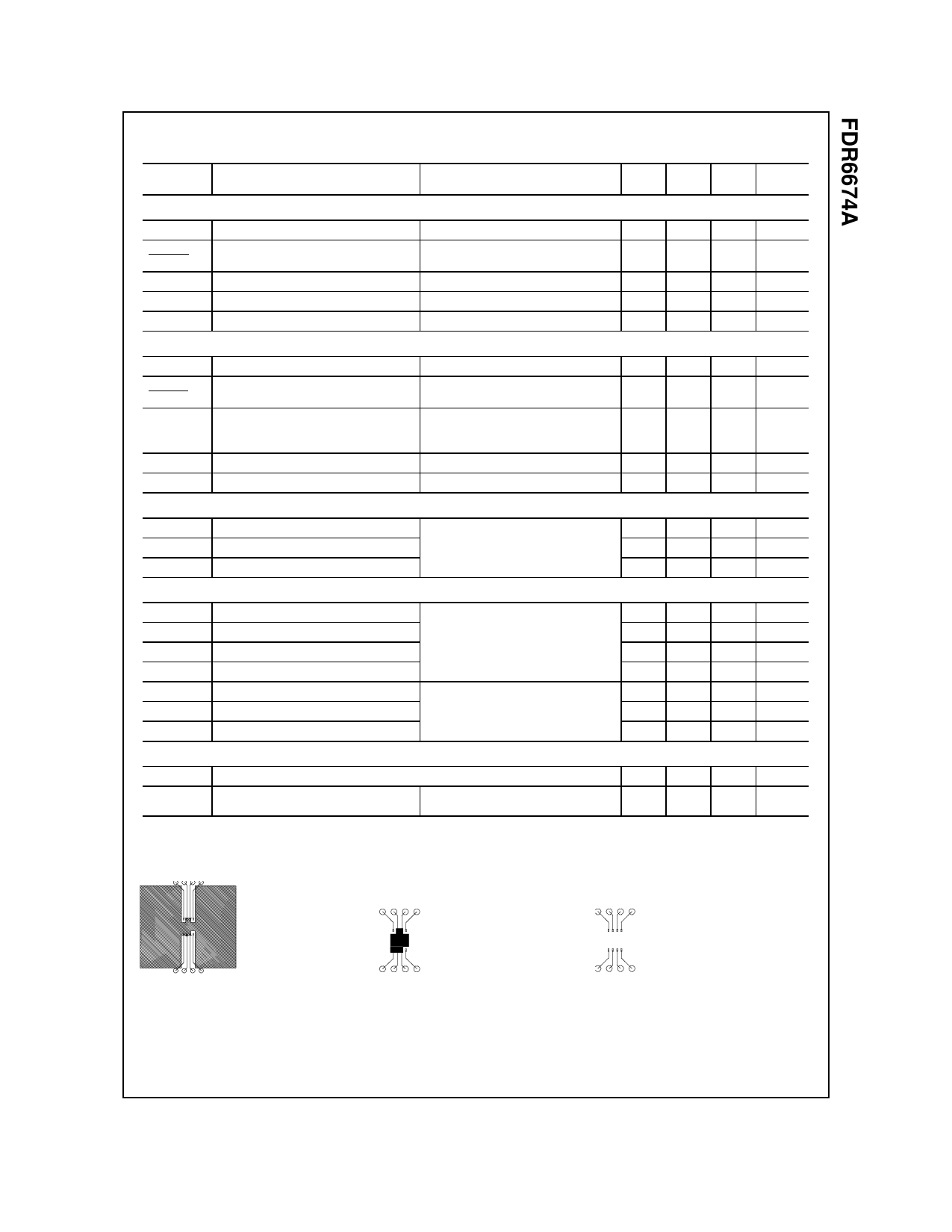
Scale 1 : 1 on letter size paper
2. Pulse Test: Pulse Width < 300Âľs, Duty Cycle < 2.0%
b) 125°/W when
mounted on a .04 in2
pad of 2 oz copper
c) 135°/W when mounted on a
minimum pad.
FDR6674A Rev D(W)
Share Link: 