7C4281V-10(2003) Ver la hoja de datos (PDF) - Cypress Semiconductor
Número de pieza
componentes Descripción
Fabricante
7C4281V-10 Datasheet PDF : 16 Pages
| |||
CY7C4261V/CY7C4271V
CY7C4281V/CY7C4291V
Switching Waveforms (continued)
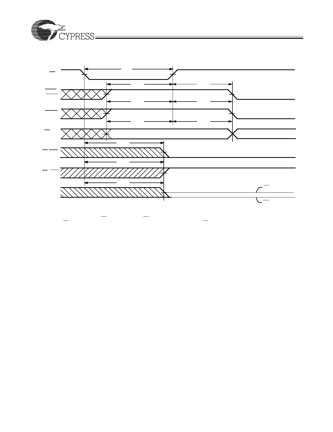
Reset Timing [14]
RS
REN1,
REN2
tRS
tRSS
tRSS
tRSR
tRSR
WEN1
tRSS
tRSR
WEN2/LD [16]
tRSF
EF,PAE
tRSF
FF, PAF
Q0 − Q8
tRSF
OE=1 [15]
OE=0
Notes:
14. The clocks (RCLK, WCLK) can be free-running during reset.
15. After reset, the outputs will be LOW if OE = 0 and three-state if OE=1.
16. Holding WEN2/LD HIGH during reset will make the pin act as a second enable pin. Holding WEN2/LD LOW during reset will make the pin act as a load enable for the
programmable flag offset registers.
Document #: 38-06013 Rev. *A
Page 9 of 16
Share Link: 