74VCX162835MTD Ver la hoja de datos (PDF) - Fairchild Semiconductor
Número de pieza
componentes Descripción
Fabricante
74VCX162835MTD
Fairchild Semiconductor

74VCX162835MTD Datasheet PDF : 8 Pages
| |||
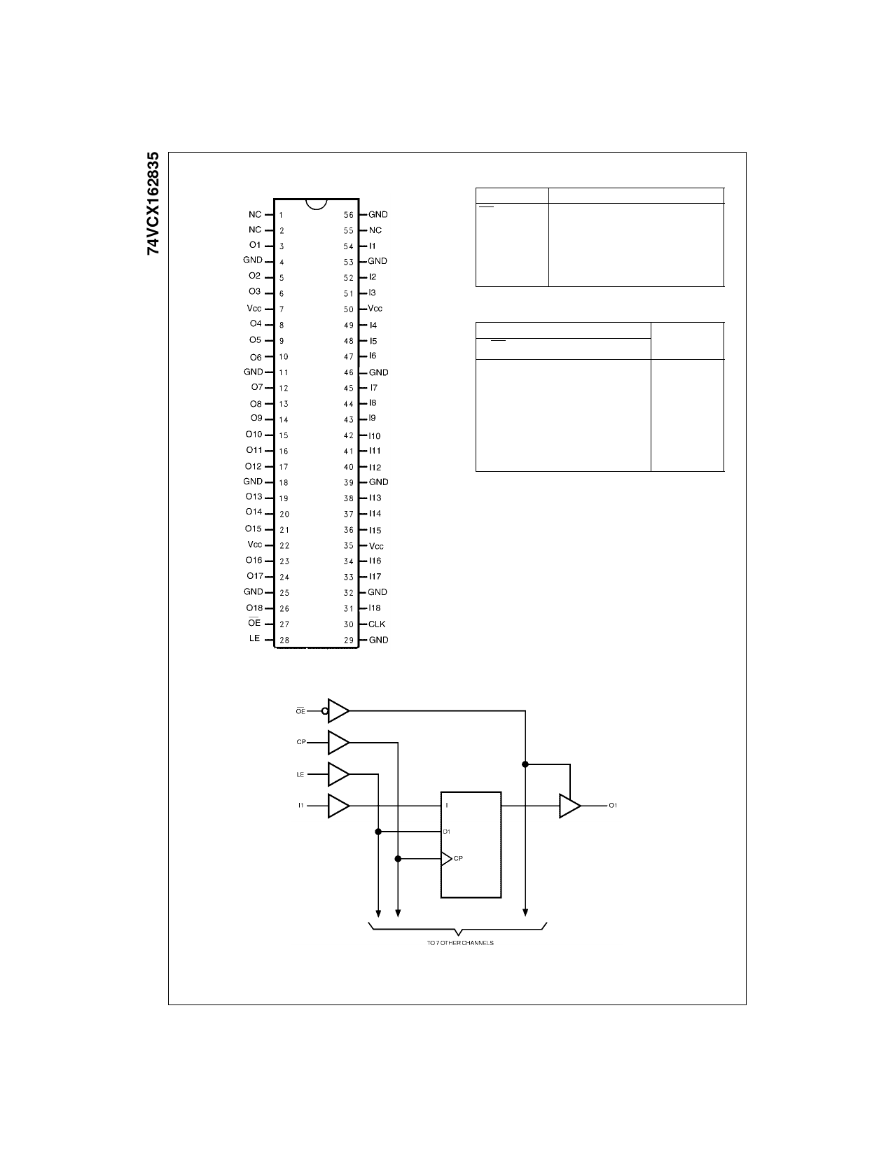
Connection Diagram
Logic Diagram
Pin Descriptions
Pin Names
OE
LE
CP
I1 - I18
O1 - O18
Description
Output Enable Input (Active LOW)
Latch Enable Input
Clock Input
Data Inputs
3-STATE Outputs
Function Table
Inputs
OE
LE
CP
In
H
X
X
X
L
H
X
L
L
H
X
H
L
L
↑
L
L
L
↑
H
L
L
H
X
L
L
L
X
H = HIGH Voltage Level
L = LOW Level Voltage
X = Immaterial (HIGH or LOW, Inputs may not float)
Z = High Impedance
Outputs
On
Z
L
H
L
H
O0 (Note 2)
O0 (Note 3)
Note 2: Output level before the indicated steady-state input conditions
were established provided that CP was HIGH before LE went LOW.
Note 3: Output level before the indicated steady-state input conditions
were established.
www.fairchildsemi.com
2
Share Link: