DP80390 Ver la hoja de datos (PDF) - Digital Core Design
Número de pieza
componentes Descripción
Fabricante
DP80390 Datasheet PDF : 10 Pages
| |||
required Wait-States depends on memory ac-
cess time and DP80390 clock frequency. In
most cases the proper number of Wait-States
cycles is between 2-5. The READY pin can be
also dynamically modulated e.g. by SDRAM
controller.
0x7FFFFF
Off chip Memory
(implemented as ROM,
SRAM or FLASH)
0x00FFFF
0x00F000
0x000400
0x000000
On chip Memory
(implemented as RAM)
Off chip Memory
(implemented as ROM,
SRAM or FLASH)
On-chip Memory
(implemented as ROM)
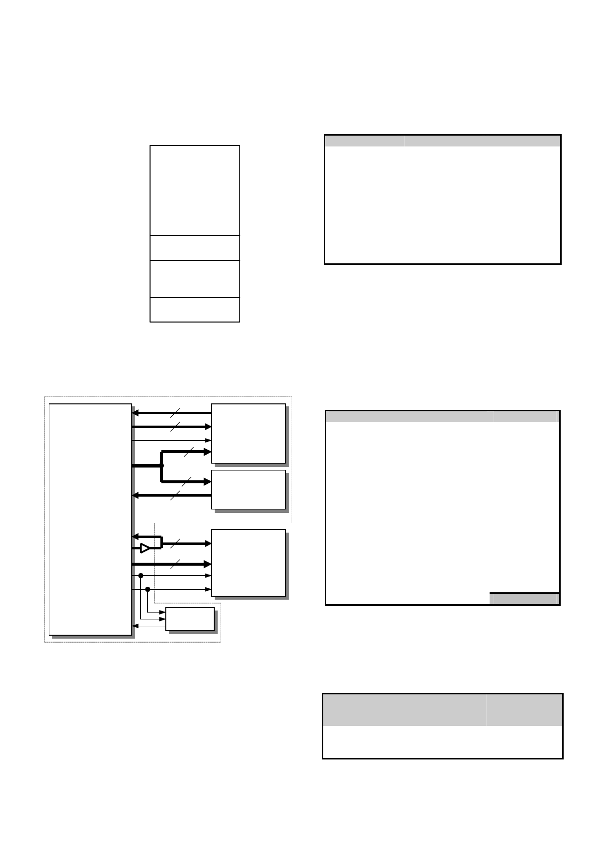
The figure below shows a typical Program
Memories connections in system with
DP80390 Microcontroller core.
PERFORMANCE
The following tables give a survey about the
Core area and performance in Programmable
Logic Devices after Place & Route (CPU fea-
tures and peripherals have been included):
Device
FLEX10KE
Speed grade
-1
Fmax
57 MHz
ACEX1K
-1
57 MHz
APEX20K
-1
50 MHz
APEX20KE
-1
66 MHz
APEX20KC
-7
78 MHz
APEX-II
-7
76 MHz
MERCURY
-5
100 MHz
CYCLONE
-6
91 MHz
CYCLONE-II
-6
93 MHz
STRATIX
-5
90 MHz
STRATIX-II
-3
160 MHz
Core performance in ALTERA® devices
For a user the most important is application
speed improvement. The most commonly used
arithmetic functions and theirs improvement
are shown in table below. Improvement was
computed as {80C51 clock periods} divided by
{DP80390 clock periods} required to execute
an identical function. More details are available
in core documentation.
prgramdatai
prgdatao
prgramwr
prgaddr
prgromdata
DP80390 i
xdatai
xdatao
xaddr
xprgrd
xprgwr
8
8
12
On-chip Memory
(implemented as RAM)
0 Wait-State access
10
8
ASIC or FPGA
chip
On-chip Memory
(implemented as ROM)
0 Wait-State access
8
Off-chip Memory
24
(implemented as
FLASH, or SRAM)
eg. 2-5 Wait-State
access
ready
Wait-States
manager
The described above implementation should be
treated as an example. All Program Memory
spaces are fully configurable. For timing-critical
applications whole program code can be imple-
mented as on-chip ROM and (or) RAM and
executed without Wait-States, but for some
other applications whole program code can be
implemented as off-chip ROM or FLASH and
executed with required number Wait-State cy-
cles.
Function
8-bit addition (immediate data)
8-bit addition (direct addressing)
8-bit addition (indirect addressing)
8-bit addition (register addressing)
8-bit subtraction (immediate data)
8-bit subtraction (direct addressing)
8-bit subtraction (indirect addressing)
8-bit subtraction (register addressing)
8-bit multiplication
8-bit division
16-bit addition
16-bit subtraction
16-bit multiplication
32-bit addition
32-bit subtraction
32-bit multiplication
Average speed improvement:
Improvement
9,00
9,00
9,00
12,00
9,00
9,00
9,00
12,00
16,00
9,60
12,00
12,00
13,60
12,00
12,00
12,60
11,12
Dhrystone Benchmark Version 2.1 was used to
measure Core performance. The following ta-
ble gives a survey about the DP80390 per-
formance in terms of Dhrystone/sec and VAX
MIPS rating.
Device
Target
Clock
fre-
quency
Dhry/sec
(VAX MIPS)
80C51
-
12 MHz
268 (0.153)
80C310
-
33 MHz 1550 (0.882)
DP8051
STRATIX-II 150 MHz 26220 (14.924)
Core performance in terms of Dhrystones
All trademarks mentioned in this document
are trademarks of their respective owners.
http://www.DigitalCoreDesign.com
http://www.dcd.pl
Copyright 1999-2007 DCD – Digital Core Design. All Rights Reserved.
Share Link: 