DP80390 Ver la hoja de datos (PDF) - Digital Core Design
Número de pieza
componentes Descripción
Fabricante
DP80390 Datasheet PDF : 10 Pages
| |||
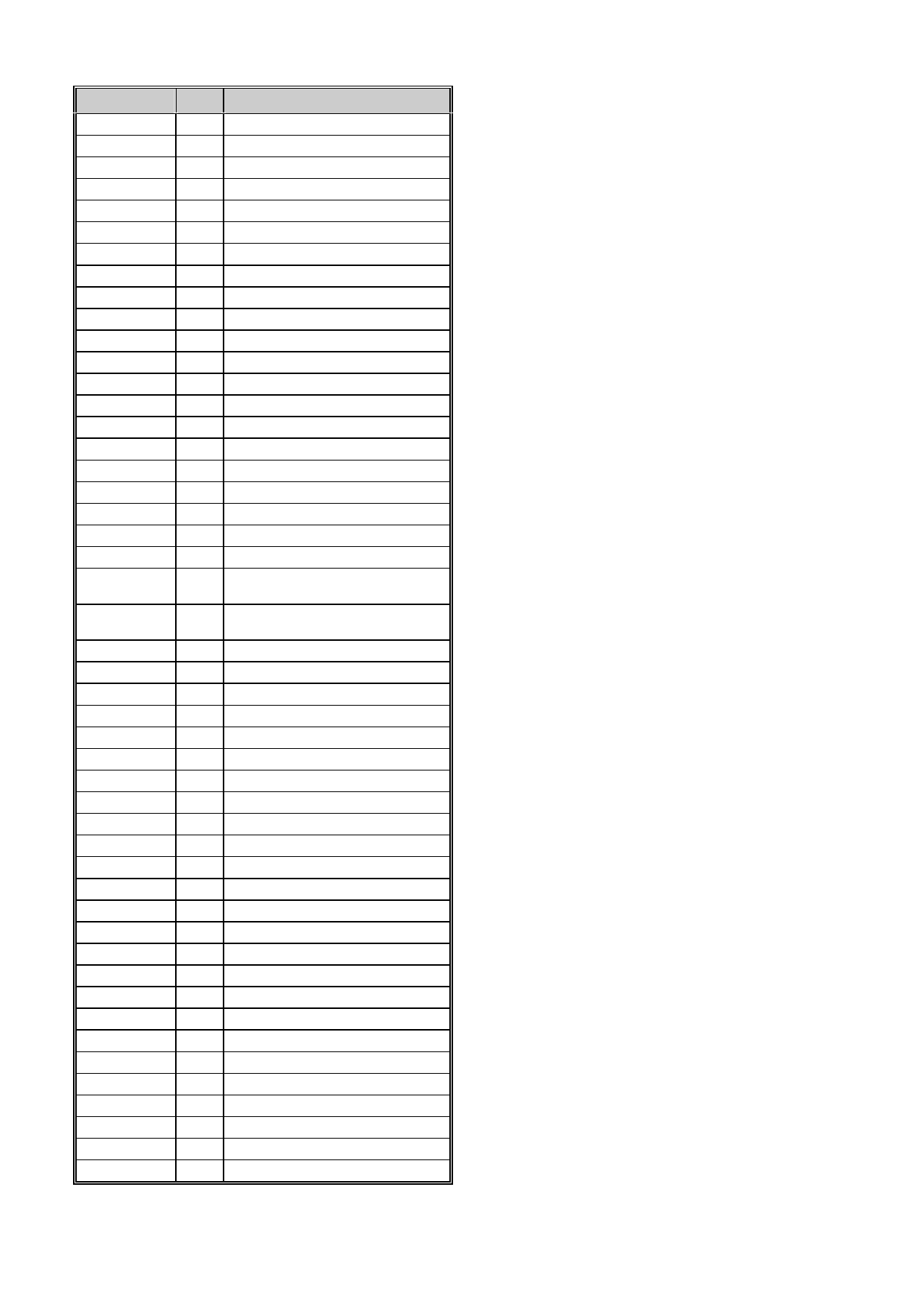
PIN
TYPE
DESCRIPTION
ready
input External memory data ready
ramdatai[7:0]
input Data bus from internal data memory
sfrdatai[7:0]
input Data bus from user SFR’s
int0
input External interrupt 0
int1
input External interrupt 1
t0
input Timer 0 input
t1
input Timer 1 input
gate0
input Timer 0 gate input
gate1
input Timer 1 gate input
rxdi
input Serial receiver input
tdi
input DoCD™ TAP data input
tck
input DoCD™ TAP clock input
tms
input DoCD™ TAP mode select input
rsto
output Reset output
port0o[7:0]
output Port 0 output
port1o[7:0]
output Port 1 output
port2o[7:0]
output Port 2 output
port3o[7:0]
output Port 3 output
prgaddr[15:0] output Internal program memory address bus
prgdatao[7:0] output Data bus for internal program memory
prgramwr
output Internal program memory write
sxdmaddr[15:0] output Sync XDATA memory address bus
(SXDM)
sxdmdatao[7:0] output Data bus for Sync XDATA memory
(SXDM)
sxdmoe
output Sync XDATA memory read (SXDM)
sxdmwe
output Sync XDATA memory write (SXDM)
xaddr[23:0]
output Address bus for external memories
xdatao[7:0]
output Data bus for external memories
xdataz
output Turn xdata bus into ‘Z’ state
xprgrd
output External program memory read
xprgwr
output External program memory write
xdatard
output External data memory read
xdatawr
output External data memory write
ramaddr[7:0] output Internal Data Memory address bus
ramdatao[7:0] output Data bus for internal data memory
ramoe
output Internal data memory output enable
ramwe
output Internal data memory write enable
sfraddr[6:0]
output Address bus for user SFR’s
sfrdatao[7:0]
output Data bus for user SFR’s
sfroe
output User SFR’s read enable
sfrwe
output User SFR’s write enable
tdo
output DoCD™ TAP data output
rtck
output DoCD™ return clock line
debugacs
output DoCD™ accessing data
coderun
output CPU is executing an instruction
pmm
output Power management mode indicator
stop
output Stop mode indicator
rxdo
output Serial receiver output
txd
output Serial transmitter output
All trademarks mentioned in this document
are trademarks of their respective owners.
UNITS SUMMARY
ALU – Arithmetic Logic Unit performs the
arithmetic and logic operations during execu-
tion of an instruction. It contains accumulator
(ACC), Program Status Word (PSW), (B) regis-
ters and related logic such as arithmetic unit,
logic unit, multiplier and divider.
Opcode Decoder – Performs an instruction
opcode decoding and the control functions for
all other blocks.
Control Unit – Performs the core synchroniza-
tion and data flow control. This module is di-
rectly connected to Opcode Decoder and
manages execution of all microcontroller tasks.
Program Memory Interface – Contains Pro-
gram Counter (PC) and related logic. It per-
forms the instructions code fetching. Program
Memory can be also written. This feature al-
lows usage of a small boot loader loading new
program into RAM, EPROM or FLASH
EEPROM storage via UART, SPI, I2C or
DoCD™ module.
External Memory Interface - Contains mem-
ory access related registers such as Data
Page High (DPH), Data Page Low (DPL) and
Data Pointer eXtended (DPX) registers. It per-
forms the external Program and Data Memory
addressing and data transfers. Program fetch
cycle length can be programmed by user. This
feature is called Program Memory Wait States,
and allows core to work with different speed
program memories.
Synchronous eXternal Data Memory
(SXDM) Interface – contains XDATA memory
access related logic allowing fast access to
synchronous memory devices. It performs the
external Data Memory addressing and data
transfers. This memory can be used to store
large variables frequently accessed by CPU,
improving overall performance of application.
Internal Data Memory Interface – Internal
Data Memory interface controls access into the
internal 256 bytes memory. It contains 8-bit
Stack Pointer (SP) register and related logic.
User SFRs Interface – Special Function Reg-
isters interface controls access to the special
registers. It contains standard and used de-
fined registers and related logic. User defined
external devices can be quickly accessed
(read, written, modified) using all direct ad-
dressing mode instructions.
http://www.DigitalCoreDesign.com
http://www.dcd.pl
Copyright 1999-2007 DCD – Digital Core Design. All Rights Reserved.
Share Link: 