RT9018A/B Ver la hoja de datos (PDF) - Richtek Technology
Número de pieza
componentes Descripción
Fabricante
RT9018A/B Datasheet PDF : 12 Pages
| |||
RT9018A/B
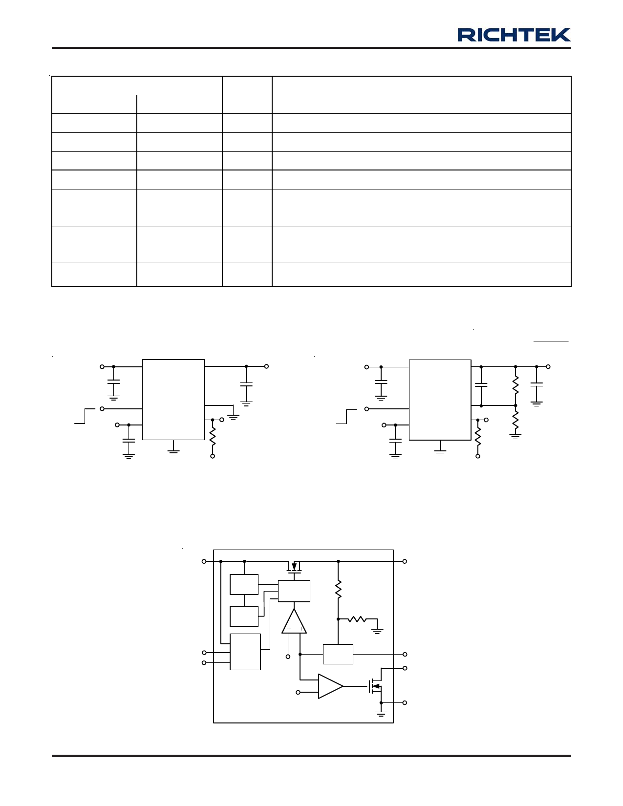
Pin Description
Pin No.
PSOP-8
WDFN 3x3
Pin Name
Pin Function
3
7, 8, 9
VIN
Supply Input Voltage.
2
6
EN
Chip Enable (Active-High).
4
10
VDD
Supply Voltage of Control Circuitry.
1
5
PGOOD Power Good Open Drain Output.
Set the output voltage by the internal feedback resistors when
7
4
ADJ
ADJ is grounded. If external feedback resistors is used, VOUT =
0.8V x (R1 + R2)/R2.
6
1, 2, 3
VOUT Output Voltage.
5
--
NC
No Internal Connection.
8,
Exposed Pad (9)
Exposed Pad (11)
GN D
Ground. The exposed pad must be soldered to a large PCB and
connected to GND for maximum power dissipation.
Typical Application Circuit
VIN
VIN
VOUT
10uF RT9018A/B
Chip Enable
VDD
EN
ADJ
VDD PGOOD
GND
1uF
100k
VOUT
VOUT
10uF
Figure 1. Fixed Voltage Regulator
VOUT
= 0.8 ×
R1+ R2
R2
VIN
VIN
VOUT
10uF RT9018A/B
CDummy R1
Chip Enable
VDD
EN
ADJ
VDD PGOOD
R2
GND
100k
1uF
VOUT
VOUT
10uF
Figure 2. Adjustable Voltage Regulator
Function Block Diagram
VIN
OCP
OTP
Driver
Error
Amplifier
EN
VDD
POR
0.8V
0.72V
Mode
-
+
VOUT
ADJ
PGOOD
GND
www.richtek.com
2
DS9018A/B-04 September 2007
Share Link: 