SSM2211_02 Ver la hoja de datos (PDF) - Analog Devices
Número de pieza
componentes Descripción
Fabricante
SSM2211_02 Datasheet PDF : 16 Pages
| |||
SSM2211
ture, as compared to an amplifier that is less efficient. This is
important when considering the amplifier device’s maximum
power dissipation rating versus ambient temperature. An inter-
nal power dissipation versus output power equation can be de-
rived to fully understand this.
The internal power dissipation of the amplifier is the internal
voltage drop multiplied by the average value of the supply cur-
rent. An easier way to find internal power dissipation is to take
the difference between the power delivered by the supply voltage
source and the power delivered into the load. The waveform of
the supply current for a bridged output amplifier is shown in
Figure 3.
VOUT
VPEAK
T
ISY
TIME
IDD, PEAK
IDD, AVG
T
TIME
Figure 3. Bridged Amplifier Output Voltage and Supply
Current vs. Time
By integrating the supply current over a period T, then dividing
the result by T, IDD,AVG can be found. Expressed in terms of
peak output voltage and load resistance:
IDD,
AVG
=
2VPEAK
pRL
(5)
therefore power delivered by the supply, neglecting the bias cur-
rent for the device is:
PSY
=
2 VDDVPEAK
pRL
(6)
Now, the power dissipated by the amplifier internally is simply
the difference between Equation 6 and Equation 3. The equa-
tion for internal power dissipated, PDISS, expressed in terms of
power delivered to the load and load resistance is:
2
PDISS =
2 ¥VDD
PL - PL
(7)
p RL
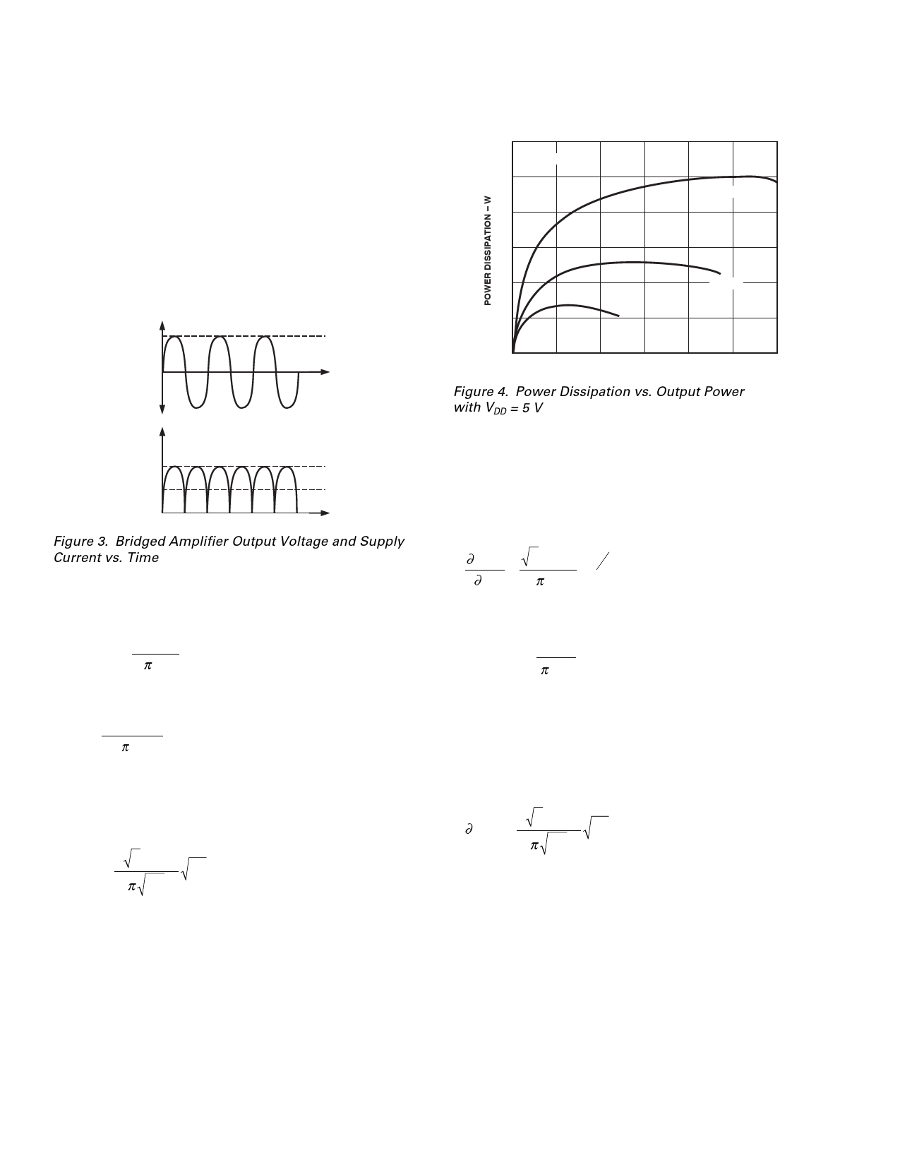
The graph of this equation is shown in Figure 4.
1.5
VDD = 5V
RL = 4⍀
1.0
0.5
RL = 8⍀
RL = 16⍀
0
0
0.5
1.0
1.5
OUTPUT POWER – W
Figure 4. Power Dissipation vs. Output Power
with VDD = 5 V
Because the efficiency of a bridged output amplifier (Equation 3
divided by Equation 6) increases with the square root of PL, the
power dissipated internally by the device stays relatively flat, and
will actually decrease with higher output power. The maximum
power dissipation of the device can be found by differentiating
Equation 7 with respect to load power, and setting the derivative
equal to zero. This yields:
∂PDISS =
∂PL
2 ¥VDD
pRL
-1
PL 2
-1=
0
(8)
And this occurs when:
2
PDISS ,MAX
=
2VDD
p 2RL
(9)
Using Equation 9 and the power derating curve in TPC 28, the
maximum ambient temperature can be easily found. This in-
sures that the SSM2211 will not exceed its maximum junction
temperature of 150∞C.
The power dissipation for a single ended output application
where the load is capacitively coupled is given by:
2
∂PDISS =
2 ¥VDD
PL - PL
p RL
(10)
The graph of Equation 10 is shown in Figure 5.
–10–
REV. B
Share Link: 