LC78622E Ver la hoja de datos (PDF) - SANYO -> Panasonic
Número de pieza
componentes Descripción
Fabricante
LC78622E Datasheet PDF : 29 Pages
| |||
LC78622E
Continued from preceding page.
Pin No.
51
52
53
54
55
56
57
58
59
60
61
62
63
64
Symbol
SBCK
FSX
WRQ
RWC
SQOUT
COIN
CQCK
RES
TST11
16M
4.2M
TEST5
CS
TEST1
I/O
Function
I Subcode readout clock input. This is a Schmitt input. (Must be connected to 0 V when unused.)
O Output for the 7.35 kHz synchronization signal divided from the crystal oscillator
O Subcode Q output standby output
I Read/write control input. This is a Schmitt input.
O Subcode Q output
I Command input from the control microprocessor
I Input for both the command input clock and the subcode readout clock. This is a Schmitt input.
I Chip reset input. This pin must be set low briefly after power is first applied.
O Test output. Leave open. (Normally outputs a low level.)
O 16.9344 MHz output.
O 4.2336 MHz output
I Test input. A pull-down resistor is built in. Must be connected to 0 V.
I Chip select input. A pull-down resistor is built in. Must be connected to 0 V if not controlled.
I Test input. No pull-down resistor. Must be connected to 0 V.
Note: The same potential must be supplied to all power supply pins, i.e., VDD, VVDD, LVDD, RVDD, and XVDD.
Pin Applications
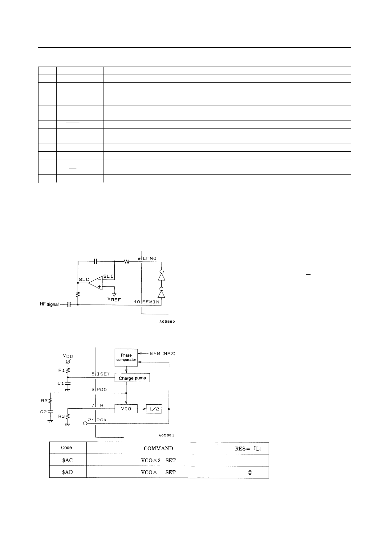
1. HF Signal Input Circuit; Pin 10: EFMIN, pin 9: EFMO, pin 1: DEFI, pin 12: CLV+
An EFM signal (NRZ) sliced at an optimal level can be acquired
by inputting the HF signal to EFMIN.
The LC78622E handles defects as follows. When a high level is
input to the DEFI pin (pin 1), EFMO (pin 9) pins (the slice level
control outputs) go to the high-impedance state, and the slice
level is held. However, note that this function is only valid in
CLV phase control mode, that is, when the V/P pin (pin 14) is
low. This function can be used in combination with the
LA9230M, LA9231M and LA9240M DEF pins.
Note: If the EFMIN and CLV+ signal lines are too close to each
other, unwanted radiation can result in error rate
degradation. We recommend laying a ground or VDD
shield line between these two lines.
2. PLL Clock Generation Circuit; Pin 3: PDO, pin 5: ISET, pin 7: FR, pin 21: PCK
Since the LC78622E includes a VCO circuit, a PLL circuit can
be formed by connecting an external RC circuit. ISET is the
charge pump reference current, PDO is the VCO circuit loop
filter, and FR is a resistor that determines the VCO frequency
range.
(Reference values)
R1 = 68 kΩ, C1 = 0.1 µF
R2 = 680 Ω, C2 = 0.1 µF
R3 = 1.2 kΩ
The VCO × 2 command is an auxiliary command for characteristics guarantee in low-voltage operations. This
command supports the low-voltage operations at VDD = 3.0 to 3.6 V.
No. 5480-8/29
Share Link: 