2N6661 Ver la hoja de datos (PDF) - Microchip Technology
Número de pieza
componentes Descripción
Fabricante
2N6661 Datasheet PDF : 10 Pages
| |||
2N6661
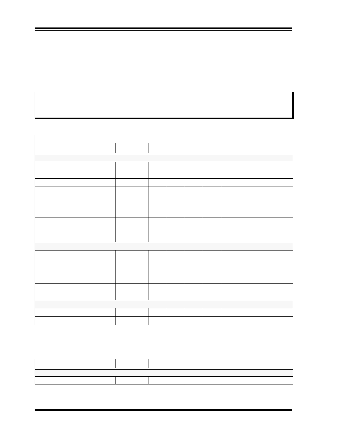
1.0 ELECTRICAL CHARACTERISTICS
ABSOLUTE MAXIMUM RATINGS†
Drain-to-source voltage ......................................................................................................................................... BVDSS
Drain-to-gate voltage.............................................................................................................................................BVDGS
Gate-to-source voltage............................................................................................................................................ ±20V
Operating and Storage Temperature .......................................................................................................... -55 to 150 °C
† Notice: Stresses above those listed under “Maximum Ratings” may cause permanent damage to the device. This is
a stress rating only and functional operation of the device at those or any other conditions above those indicated in the
operational listings of this specification is not implied. Exposure to maximum rating conditions for extended periods
may affect device reliability.
ELECTRICAL CHARACTERISTICS
Electrical Specifications: Unless otherwise specified, for all specifications TA = +25°C
Parameter
Symbol
Min Typ Max Units Conditions
DC Parameters (Note 1, unless otherwise stated)
Drain-to-source breakdown voltage
Gate threshold voltage
VGS(th) change with temperature
Gate body leakage current
Zero gate voltage drain current
BVDSS
VGS(th)
∆VGS(th)
IGSS
IDSS
On-state drain current
Static drain-to-source on-state
resistance
AC Parameters (Note 2)
ID(ON)
RDS(ON)
90
-
-
V VGS= 0V, ID= 10µA
0.8
-
2.0
V VGS= VDS, ID= 1.0mA
-
-3.8 -5.5 mV/°C VGS= VDS, ID= 1.0mA (Note 2)
-
-
100 nA VGS= ±20V, VDS= 0V
-
-
10
µA VGS= 0V, VDS= Max rating
-
-
500
VDS= 0.8 Max Rating,
VGS= 0V, TA= 125°C (Note 2)
1.5
-
-
A VGS= 10V, VDS= 10V
-
-
5.0
Ω VGS= 5.0V, ID= 0.3A
-
-
4.0
VGS= 10V, ID= 1.0A
Forward transconductance
Input capacitance
Common source output capacitance
Reverse transfer capacitance
Turn-on time
Turn-off time
Diode Parameters
GFS
CISS
COSS
CRSS
t(ON)
t(OFF)
170
-
-
-
-
-
-
-
-
-
-
-
- mmho VDS= 25V, ID= 0.5A
50
pF VGS= 0V,
40
VDS= 24V,
f = 1.0MHz
10
10
ns VDD= 25V, ID= 1.0A,
10
RGEN= 25Ω
Diode forward voltage drop
VSD
-
1.2
-
V VGS= 0V, ISD= 1.0A (Note 1)
Reverse recovery time
trr
-
350
-
ns VGS= 0V, ISD= 1.0A (Note 2)
Note 1: All DC parameters are 100% tested at 25°C unless otherwise stated. Pulse test: 300 µs pulse, 2% duty cycle.
2: Specification is obtained by characterization and is not 100% tested.
TEMPERATURE SPECIFICATIONS
Parameter
Symbol
Temperature Ranges
Operating and Storage Temperature
TA
Min Typ Max Units Conditions
-55
–
150 °C
DS20005516A-page 2
2016 Microchip Technology Inc.
Share Link: 