LA4625-E Ver la hoja de datos (PDF) - ON Semiconductor
Número de pieza
componentes Descripción
Fabricante
LA4625-E Datasheet PDF : 8 Pages
| |||
LA4625
Pin Voltages
VCC = 12V, with 5V applied to STBY through a 10kΩ resistor, RL = 4Ω, Rg = 0
Pin No.
1
2
3
4
5
Pin name
IN1
DC
PRE-GND
STBY
ON TIME
Pin voltage
1.46V
5.18V
0V
3.21V
2.26V
6
IN2
1.46V
7
POP
2.05V
Pin No.
Pin name
Pin voltage
8
+OUT2
5.21V
9
−OUT2
5.21V
10
PWR-GN
0V
11
+OUT1
5.21V
12
PWR-GN
0V
13
−OUT1
5.21V
14
VCC
12V
External Components
C1 and C4: Input capacitors. A value of 2.2μF is recommended. Determine the polarity based on the DC potential of
the circuit connected directly to the LA4625 front end. Note that the low band response can be adjusted by
varying fL with the capacitors C1 and C4.
C2
: Decoupling capacitor (ripple filter)
C3
: Sets the amplifier starting time, which will be approximately 0.6 seconds for a value of 33μF. The starting
time is proportional to the value of this capacitor, and can be set to any desired value.
C5
: Power-supply capacitor
C6, C7, C8, and C9 :
Oscillation prevention capacitors. Use polyester film capacitors (Mylar capacitors) with excellent
characteristics. (Note that the series resistors R2, R3, R4, and R5 are used in conjunction with these
capacitors to achieve stable amplifier operation.) A value of 0.1μF is recommended.
C10 : Impulse noise reduction capacitor. A value of 0.47μF is recommended. Caution is required when selecting
the value for this capacitor, since increasing its value influences the operation of the circuits that protect
against shorting the amplifier output pins to VCC or to ground when higher VCC voltages (approximately
16V or higher) are used.
R1
: Standby switch current limiting resistor. A value of 10kΩ is recommended when a voltage in the range 2.5 to
12V will be applied as the standby switching voltage. Note that this resistor is not optional: it must be included.
IC Internal Characteristics and Notes
1. Standby function
• Pin 4 is the standby switch. A voltage of 2.5V or
higher must be applied through an external resistor to
turn the amplifier on.
• If a voltage of over 12V will be applied as the
standby mode switching voltage, use the following
formula to determine the value of R1 so that the
current entering at pin 4 remains under 500μA.
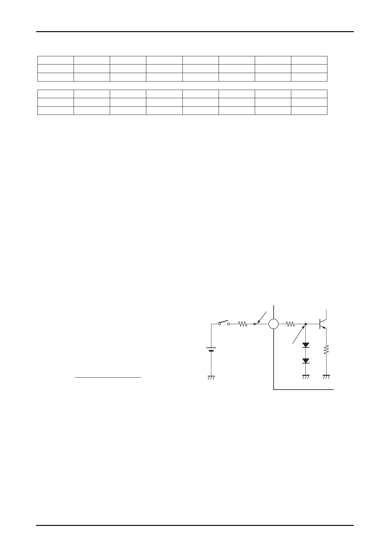
Pin 4 Internal Equivalent Circuit
500μA or lower
4
R1
10kΩ
Applied standby
voltage
About 1.4V
(2VBE)
R1 =
<applied voltage> − 1.4
500μA
− 10kΩ
2. Muting function
• Pin 5 connects the capacitor that determines the starting time to prevent impulse noise. It can also be used to mute
the amplifier output by shorting pin 5 to ground. When this function is used, the recovery time depends on C3.
3. Impulse noise improvements
• While the LA4625 achieves a low level of impulse noise, if even further reductions in impulse noise at power
on/off (and when switching into or out of standby mode) a 0.47μF capacitor may be inserted between pin 7 and the
PRE GND pin (pin 3). (Pin 7 is the output amplifier bias pin. Since the ability to withstand shorting the output pins
to VCC or ground is reduced for supply voltages over 16V if the pin 7 capacitance is large, we recommend a value
of 0.47μF or lower for this capacitor.)
No.6631-4/8
Share Link: 