5L35021 Ver la hoja de datos (PDF) - Integrated Device Technology
NГєmero de pieza
componentes DescripciГіn
Fabricante
5L35021 Datasheet PDF : 37 Pages
| |||
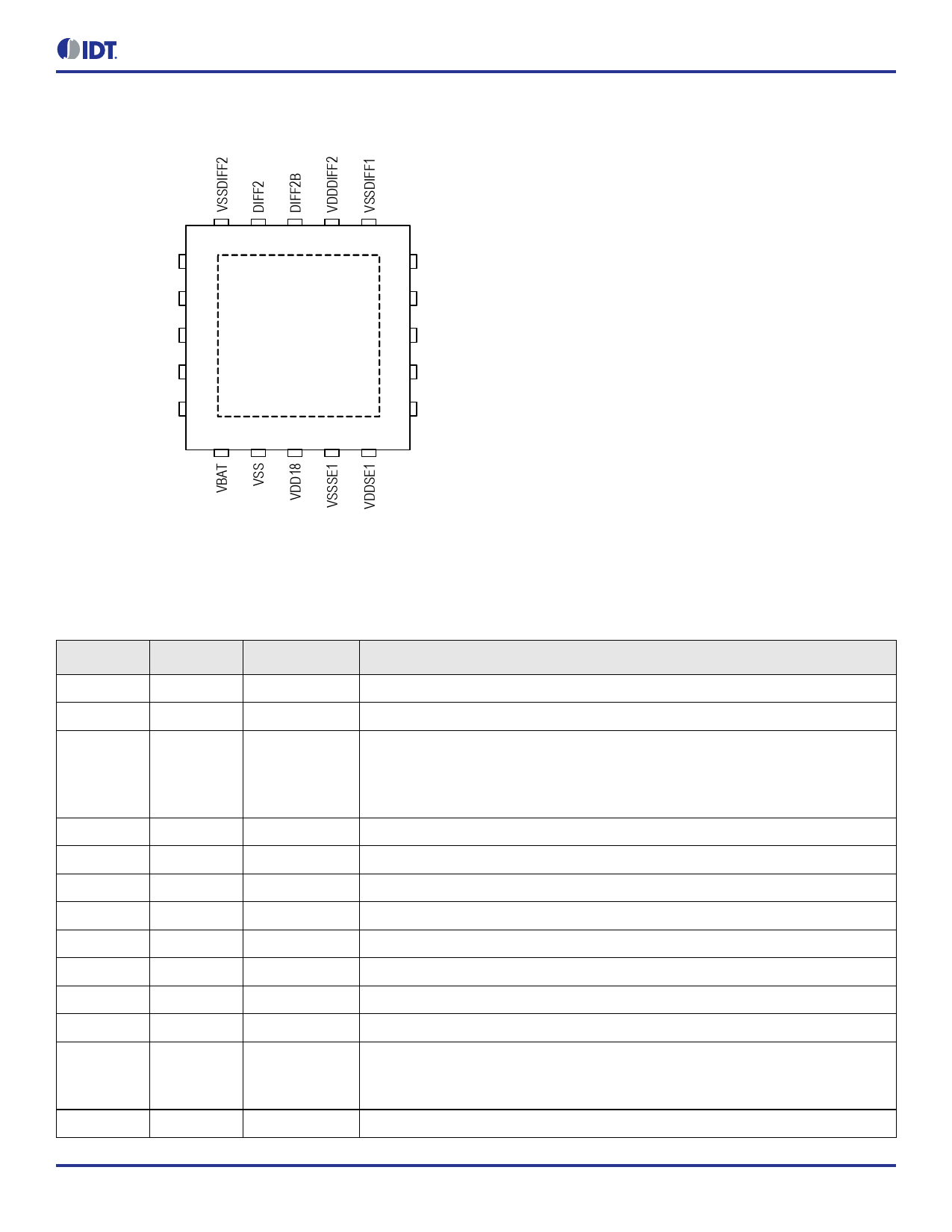
Pin Assignments
Figure 1. Pin Assignments for 3 x 3 mm 20-VFQFPN Package – Top View
5L35021 Datasheet
20 19 18 17 16
VDDA 1
15 DIFF1
SDA_DFCO 2
SEL_DFC/SCL_DFC1 3
5L35021
14 DIFF1B
13 VDDDIFF1
CLKIN/X2 4
12 OE1
CLKINB/X1 5
11 SE1
6
7
89
10
3 x 3 mm 20-QFN
Pin Descriptions
Table 1. Pin Descriptions
Number
1
2
Name
VDDA
SDA_DFC0
Type
Power
I/O
3
SEL_DFC/
SCL_DFC1
Input
4
CLKIN/X2
I/O
5
CLKINB/X1
Input
6
VBAT
Power
7
VSS
Power
8
VDD18
Power
9
VSSSE1
Power
10
VDDSE1
Power
11
SE1
Output
12
OE1
Input
13
VDDDIFF1
Power
Description
VDD 1.8V
I2C data pin. The pin can be DFC0 function by pin 3 SEL_DFC power-on latch status.
I2C CLK pin.
SEL_DFC is a latch input pin during the power-up.
High on power-on: I2C mode as SCLK function.
Low on power-on: pin 3 SCL and pin 2 SDA as DFC function control pins.
Crystal oscillator interface output or differential clock input pin (CLKIN).
Crystal oscillator interface input or differential clock input pin (CLKINB).
Power supply pin for 32.768kHz DCO; usually connect to coin cell battery, 1.8V.
Connect to ground.
VDD 1.8V.
Connect to ground.
Output power supply. Connect to 1.8V. Sets output voltage levels for SE1.
Output clock SE1.
OE1’s function selected from OTP pre-programmed register bits.
OE1 pull to 6.5V when burn OTP registers.
Refer to OE Pin Functions table for details.
Output power supply. Connect to 1.8V. Sets output voltage levels for DIFF1.
В©2017 Integrated Device Technology, Inc.
2
July 13, 2017
Share Link: 