5L35021 Ver la hoja de datos (PDF) - Integrated Device Technology
N√∫mero de pieza
componentes Descripción
Fabricante
5L35021 Datasheet PDF : 37 Pages
| |||
5L35021 Datasheet
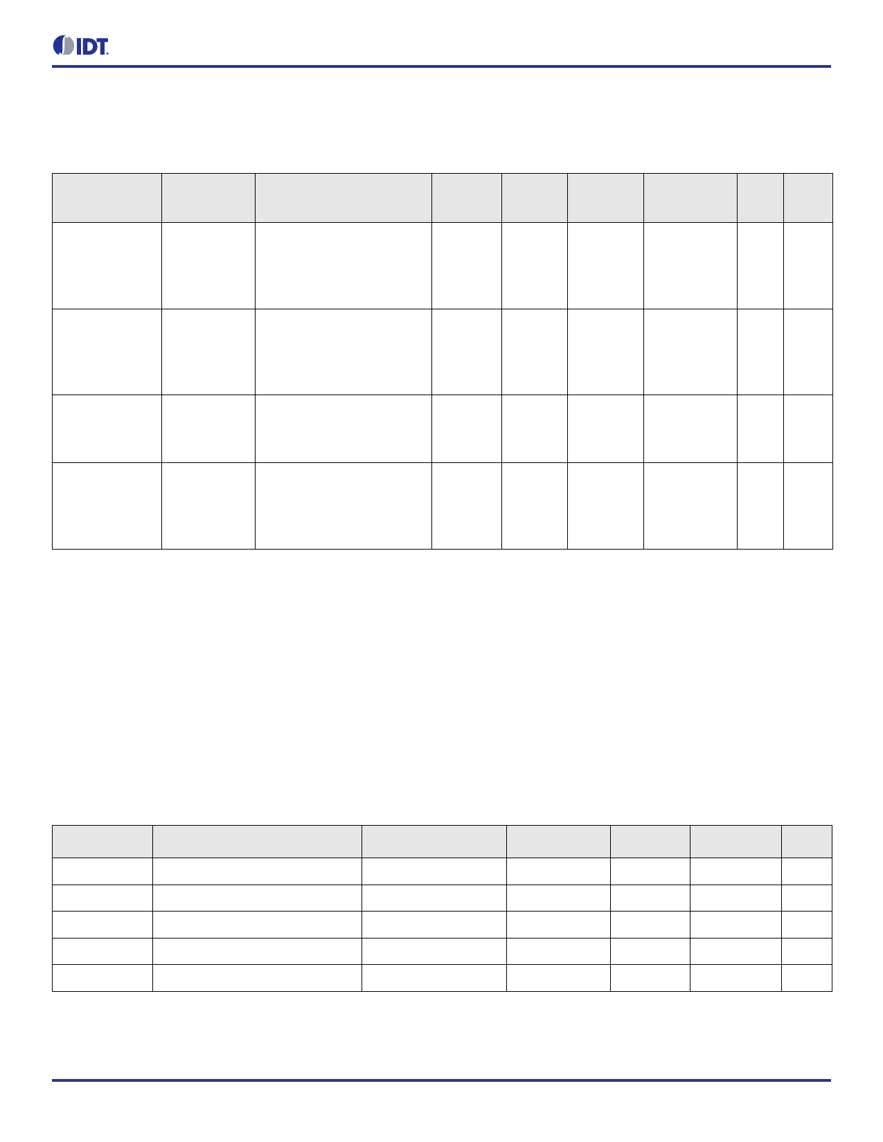
PCI Express Jitter Specifications
VDDDIFF = 1.8V ±5% TA = -40°C to +85°C
Table 11. PCI Express Jitter Specifications
Symbol
Parameter
Conditions
Minimum
tJ (PCIe Gen1)
tREFCLK_HF_RMS
(PCIe Gen2)
tREFCLK_LF_RMS
(PCIe Gen2)
tREFCLK_RMS
(PCIe Gen3)
Phase Jitter
Peak-to-Peak
Phase Jitter
RMS
Phase Jitter
RMS
Phase Jitter
RMS
ƒ = 100MHz/125MHz,
25MHz crystal input.
Evaluation band: 0Hz –
Nyquist (clock frequency/2).
ƒ = 100MHz/125MHz,
25MHz crystal input.
High band: 1.5MHz –
Nyquist (clock frequency/2).
ƒ = 100MHz/125MHz,
25MHz crystal input.
Low band: 10kHz – 1.5MHz.
ƒ = 100MHz/125MHz,
25MHz crystal input.
Evaluation band: 0Hz –
Nyquist (clock frequency/2).
Typical
27
1.9
0.9
0.5
Industry
Maximum Specification Units Notes
86
ps 1,4
3.10
ps 2,4
3.0
ps 2,4
1.0
ps 3,4
Note: Electrical parameters are guaranteed over the specified ambient operating temperature range, which is established when the device is mounted
in a test socket with maintained transverse airflow greater than 500 lfpm. The device will meet specifications after thermal equilibrium has been
reached under these conditions.
1 Peak-to-peak jitter after applying system transfer function for the common clock architecture. Maximum limit for PCI Express Gen1.
2 RMS jitter after applying the two evaluation bands to the two transfer functions defined in the common clock architecture and reporting the worst
case results for each evaluation band. Maximum limit for PCI Express Gen2 is 3.1ps RMS for tREFCLK_HF_RMS (high band) and 3.0ps RMS for
tREFCLK_LF_RMS (low band).
3 RMS jitter after applying system transfer function for the common clock architecture. This specification is based on the PCI_Express_Base_r3.0 10
Nov. 2010 specification, and is subject to change pending the final release version of the specification.
4 This parameter is guaranteed by characterization. Not tested in production.
I2C Bus Characteristics
Table 12. I2C Bus DC Characteristics
Symbol
VIH
VIL
VHYS
IIN
VOL
Parameter
Input High Level
Input Low Level
Hysteresis of Inputs
Input Leakage Current
Output Low Voltage
Conditions
IOL = 3mA.
Minimum
0.7 √ó VDD18
0.05 √ó VDD18
Typical
Maximum
0.3 √ó VDD18
±1
0.4
Units
V
V
V
μA
V
©2017 Integrated Device Technology, Inc.
10
July 13, 2017
Share Link: 