LT1585-1.5 Ver la hoja de datos (PDF) - Linear Technology
Número de pieza
componentes Descripción
Fabricante
LT1585-1.5 Datasheet PDF : 8 Pages
| |||
LT1585-1.5/LT1585A-1.5
APPLICATIONS INFORMATION
Load Regulation
It is not possible to provide true remote load sensing
because the LT1585-1.5/LT1585A-1.5 are 3-terminal de-
vices. Load regulation is limited by the resistance of the
wire connecting the regulators to the load. Load regulation
per the data sheet specification is measured at the bottom
of the package.
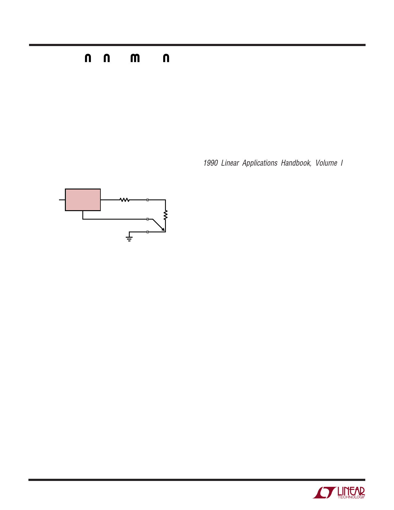
For fixed voltage devices, negative side sensing is a true
Kelvin connection with the GND pin of the device returned
to the negative side of the load. This is illustrated in
Figure 3.
LT1585-1.5
RP
PARASITIC
LINE RESISTANCE
VIN IN
OUT
GND
RL
1585-1.5 F03
Figure 3. Connection for Best Load Regulation
Thermal Considerations
The LT1585-1.5/LT1585A-1.5 protect the device under
overload conditions with internal power and thermal limit-
ing circuitry. However, for normal continuous load condi-
tions, do not exceed maximum junction temperature rat-
ings. It is important to consider all sources of thermal
resistance from junction-to-ambient. These sources in-
clude the junction-to-case resistance, the case-to-heat
sink interface resistance, and the heat sink resistance.
Thermal resistance specifications have been developed to
more accurately reflect device temperature and ensure safe
operating temperatures. The electrical characteristics sec-
tion provides a separate thermal resistance and maximum
junction temperature for both the control circuitry and the
power transistor. Older regulators with a single junction-
to-case thermal resistance specification, use an average of
the two values provided here and allow excessive junction
temperatures under certain conditions of ambient tem-
perature and heat sink resistance. Calculate the maximum
junction temperature for both sections to ensure that both
thermal limits are met.
Junction-to-case thermal resistance is specified from the
IC junction to the bottom of the case directly below the die.
This is the lowest resistance path for heat flow. Proper
mounting ensures the best thermal flow from this area of
the package to the heat sink. Linear Technology strongly
recommends thermal compound at the case-to-heat sink
interface. Use a thermally conductive spacer if the case of
the device must be electrically isolated and include its
contribution to the total thermal resistance. Please consult
“Mounting Considerations for Power Semiconductors”
1990 Linear Applications Handbook, Volume I, Pages
RR3-1 to RR3-20. The output connects to the case of the
device in the LT1585-1.5/LT1585A-1.5.
For example, using an LT1585ACT-1.5 (TO-220, commer-
cial) and assuming:
VIN (Max Continuous) = 3.465V (3.3V + 5%), VOUT = 1.5V
IOUT = 5A
TA = 70°C, θHEAT SINK = 3°C/W
θCASE-TO-HEAT SINK = 1°C/W (with Thermal Compound)
Power dissipation under these conditions is equal to:
PD = (VIN – VOUT)(IOUT) = (3.465 – 1.5)(5A) = 9.825W
Junction temperature will be equal to:
TJ = TA + PD(θHEAT SINK + θCASE-TO-HEAT SINK + θJC)
For the Control Section:
TJ = 70°C + 9.825W (3°C/W + 1°C/W + 0.7°C/W) = 116.2°C
116.2°C < 125°C = TJMAX (Control Section Commercial
Range)
For the Power Transistor:
TJ = 70°C + 9.825W (3°C/W + 1°C/W + 3°C/W) = 138.8°C
138.8°C < 150°C = TJMAX (Power Transistor Commercial
Range)
In both cases the junction temperature is below the maxi-
mum rating for the respective sections, ensuring reliable
operation.
6
Share Link: 