LTC1416 Ver la hoja de datos (PDF) - Linear Technology
Número de pieza
componentes Descripción
Fabricante
LTC1416 Datasheet PDF : 20 Pages
| |||
LTC1416
APPLICATIONS INFORMATION
Input Filtering
The noise and the distortion of the input amplifier and
other circuitry must be considered since they will add to
the LTC1416 noise and distortion. The small-signal band-
width of the sample-and-hold circuit is 15MHz. Any noise
or distortion products that are present at the analog inputs
will be summed over this entire bandwidth. Noisy input
circuitry should be filtered prior to the analog inputs to
minimize noise. A simple 1-pole RC filter is sufficient for
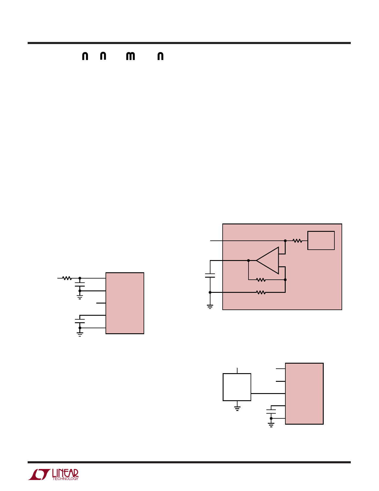
many applications. For example, Figure 7 shows a 1000pF
capacitor from AIN+ to ground and a 200Ω source resistor
to limit the input bandwidth to 800kHz. The 1000pF
capacitor also acts as a charge reservoir for the input
sample-and-hold and isolates the ADC input from sam-
pling glitch sensitive circuitry. High quality capacitors and
resistors should be used since these components can add
distortion. NPO and silver mica type dielectric capacitors
have excellent linearity. Carbon surface mount resistors
can also generate distortion from self-heating and from
damage that may occur during soldering. Metal film
surface mount resistors are much less susceptible to both
problems.
ANALOG 200Ω
INPUT
1 AIN+
1000pF
2 AIN–
3
LTC1416
VREF
22µF
4
REFCOMP
5
AGND
1416 F07
accommodate other input ranges often with little or no
additional circuitry. The following sections describe the
reference and input circuitry and how they affect the input
range.
Internal Reference
The LTC1416 has an on-chip, temperature compensated,
curvature corrected, bandgap reference that is factory
trimmed to 2.500V. It is connected internally to a reference
amplifier and is available at VREF (Pin 3). See Figure 8a. A
4k resistor is in series with the output so that it can be
easily overdriven by an external reference or other cir-
cuitry (see Figure 8b). The reference amplifier gains the
voltage at the VREF pin by 1.625 to create the required
internal reference voltage. This provides buffering be-
tween the VREF pin and the high speed capacitive DAC. The
3 VREF
2.5V
4.0625V 4 REFCOMP
22µF
5 AGND
REF
AMP
R2
80k
R3
128k
R1
4k
BANDGAP
REFERENCE
LTC1416
1416 F08a
Figure 8a. LTC1416 Reference Circuit
Figure 7. RC Input Filter
Input Range
The ±2.5V input range of the LTC1416 is optimized for low
noise and low distortion. Most op amps also perform best
over this same range, allowing direct coupling to the
analog inputs and eliminating the need for special transla-
tion circuitry.
Some applications may require other input ranges. The
LTC1416 differential inputs and reference circuitry can
5V
VIN
LT1019A-2.5
VOUT
ANALOG
INPUT
22µF
1 AIN+
2 AIN–
3
LTC1416
VREF
4
REFCOMP
5
AGND
1416 F08b
Figure 8b. Using the LT1019-2.5 as an External Reference
11
Share Link: 