LT1677CS8 Ver la hoja de datos (PDF) - Linear Technology
Número de pieza
componentes Descripción
Fabricante
LT1677CS8 Datasheet PDF : 16 Pages
| |||
LT1677
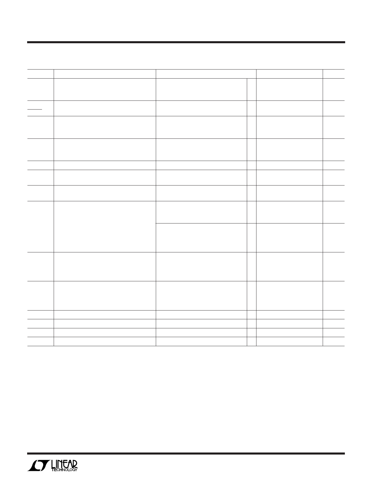
ELECTRICAL CHARACTERISTICS The q denotes the specifications which apply over the temperature range of
– 40°C < TA < 85°C. VS = ±15V, VCM = VO = 0V unless otherwise noted. (Note 5)
SYMBOL
VOS
PARAMETER
Input Offset Voltage
∆VOS
∆Temp
IB
Average Input Offset Drift
Input Bias Current
IOS
Input Offset Current
VCM
CMRR
PSRR
AVOL
Input Voltage Range
Common Mode Rejection Ratio
Power Supply Rejection Ratio
Large-Signal Voltage Gain
VOL
Output Voltage Swing Low
VOH
Output Voltage Swing High
ISC
Output Short-Circuit Current (Note 3)
SR
Slew Rate
GBW
Gain Bandwidth Product
IS
Supply Current
CONDITIONS (Note 6)
VCM = 14.0V to 14.7V
VCM = –13.3V to –15V
SO-8
N8 (Note 10)
VCM = 14.0V to 14.7V
VCM = –13.3V to –15V
VCM = 14.0V to 14.7V
VCM = –13.3V to –15V
VCM = –13.3V to 14.0V
VCM = –15V to 14.7V
VS = ±1.7V to ±18V
VS = 3.1V to 40V, VCM = VO = 1.7V
RL ≥ 10k, VO = ±14V
RL ≥ 1k, VO = ±13.5V
RL ≥ 600Ω, VO = ±10V
VCC = 5V or 3V, VEE = 0V, VCM = 1.7V,
VOUT = 0.5V to:
RL ≥ 10k, VCC – 0.5V
RL ≥ 1k, VCC – 0.7V
Above VEE
ISINK = 0.1mA
ISINK = 2.5mA
ISINK = 10mA
Below VCC
ISOURCE = 0.1mA
ISOURCE = 2.5mA
ISOURCE = 10mA
RL ≥ 10k (Note 9)
fO = 100kHz
MIN TYP MAX
q
45
180
q
200 650
q
2
6.5
q
0.40
2.0
q
0.20
0.5
q
±7
± 50
q
0.25 0.75
q – 2.3 – 0.45
q
6
40
q
100 250
q
100 400
q –15
14.7
q 105
124
q 72
91
q 103
125
q 105
120
q
3
17
q 1.5
8
q 0.2
0.35
q
2
15
q 0.2
2
q
90
230
q
175 350
q
450 650
q
150 250
q
250 375
q
600 850
q 18
25
q 1.2
2.0
q
5.8
q
3.1
4.0
UNITS
µV
µV
mV
µV/°C
µV/°C
nA
µA
µA
nA
nA
nA
V
dB
dB
dB
dB
V/µV
V/µV
V/µV
V/µV
V/µV
mV
mV
mV
mV
mV
mV
mA
V/µs
MHz
mA
Note 1: Absolute Maximum Ratings are those values beyond which the life
of the device may be impaired.
Note 2: The inputs are protected by back-to-back diodes. Current limiting
resistors are not used in order to achieve low noise. If differential input
voltage exceeds ±1.4V, the input current should be limited to 25mA. If the
common mode range exceeds either rail, the input current should be
limited to 10mA.
Note 3: A heat sink may be required to keep the junction temperature
below absolute maximum.
Note 4: The LT1677C and LTC1677I are guaranteed functional over the
Operating Temperature Range of – 40°C to 85°C.
Note 5: The LT1677C is guaranteed to meet specified performance from
0°C to 70°C. The LT1677C is designed, characterized and expected to
meet specified performance from –40°C to 85°C but is not tested or QA
sampled at these temperatures. The LT1677I is guaranteed to meet the
extended temperature limits.
Note 6: Typical parameters are defined as the 60% yield of parameter
distributions of individual amplifier; i.e., out of 100 LT1677s, typically 60
op amps will be better than the indicated specification.
Note 7: See the test circuit and frequency response curve for 0.1Hz to
10Hz tester in the Applications Information section of the LT1677 data
sheet.
Note 8: Noise is 100% tested.
Note 9: Slew rate is measured in AV = – 1; input signal is ±7.5V, output
measured at ±2.5V.
Note 10: This parameter is not 100% tested.
5
Share Link: 