LT1677CS8 Ver la hoja de datos (PDF) - Linear Technology
Número de pieza
componentes Descripción
Fabricante
LT1677CS8 Datasheet PDF : 16 Pages
| |||
LT1677
APPLICATIO S I FOR ATIO
Offset Voltage and Drift
Thermocouple effects, caused by temperature gradients
across dissimilar metals at the contacts to the input
terminals, can exceed the inherent drift of the amplifier
unless proper care is exercised. Air currents should be
minimized, package leads should be short, the two input
leads should be close together and maintained at the same
temperature.
The circuit shown to measure offset voltage is also used
as the burn-in configuration for the LT1677, with the
supply voltages increased to ±20V (Figure 4).
creating additional phase shift and reducing the phase
margin. A small capacitor (20pF to 50pF) in parallel with RF
will eliminate this problem.
RF
–
+
LT1677
OUTPUT
Figure 5. Pulsed Operation
2.5V/µs
1677 F05
50k*
15V
2–
7
100Ω* LT1677
3+
4
50k*
–15V
6
VOUT
VOUT = 1000VOS
*RESISTORS MUST HAVE LOW
THERMOELECTRIC POTENTIAL
1677 F04
Figure 4. Test Circuit for Offset Voltage and
Offset Voltage Drift with Temperature
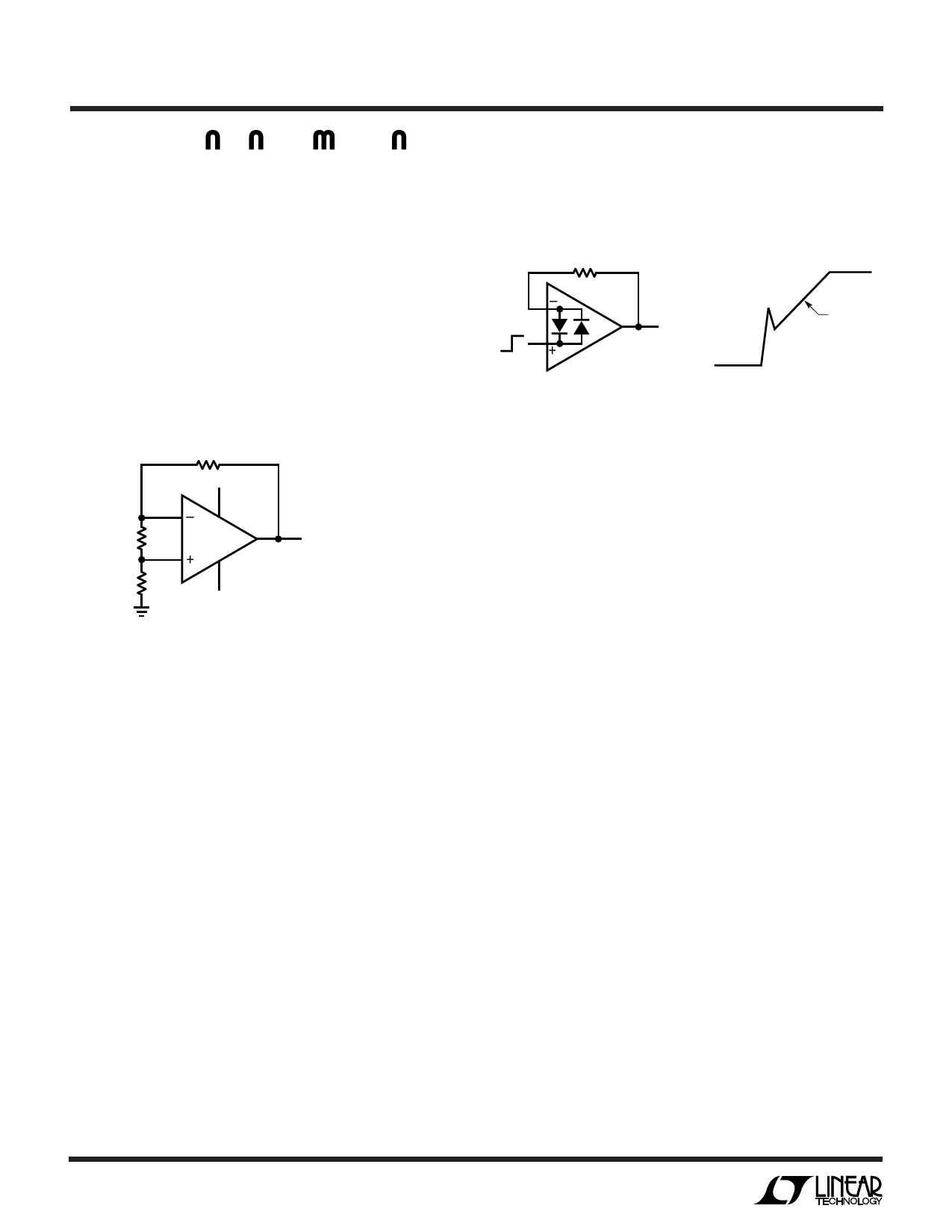
Unity-Gain Buffer Application
When RF ≤ 100Ω and the input is driven with a fast, large-
signal pulse (>1V), the output waveform will look as
shown in the pulsed operation diagram (Figure 5).
During the fast feedthrough-like portion of the output, the
input protection diodes effectively short the output to the
input and a current, limited only by the output short-circuit
protection, will be drawn by the signal generator. With
RF ≥ 500Ω, the output is capable of handling the current
requirements (IL ≤ 20mA at 10V) and the amplifier stays
in its active mode and a smooth transition will occur.
As with all operational amplifiers when RF > 2k, a pole will
be created with RF and the amplifier’s input capacitance,
Noise Testing
The 0.1Hz to 10Hz peak-to-peak noise of the LT1677 is
measured in the test circuit shown (Figure 6a). The fre-
quency response of this noise tester (Figure 6b) indicates
that the 0.1Hz corner is defined by only one zero. The test
time to measure 0.1Hz to 10Hz noise should not exceed
ten seconds, as this time limit acts as an additional zero to
eliminate noise contributions from the frequency band
below 0.1Hz.
Measuring the typical 70nV peak-to-peak noise perfor-
mance of the LT1677 requires special test precautions:
1. The device should be warmed up for at least five
minutes. As the op amp warms up, its offset voltage
changes typically 3µV due to its chip temperature
increasing 10°C to 20°C from the moment the power
supplies are turned on. In the ten-second measurement
interval these temperature-induced effects can easily
exceed tens of nanovolts.
2. For similar reasons, the device must be well shielded
from air currents to eliminate the possibility of
thermoelectric effects in excess of a few nanovolts,
which would invalidate the measurements.
3. Sudden motion in the vicinity of the device can also
“feedthrough” to increase the observed noise.
10
Share Link: 