RC4153 Ver la hoja de datos (PDF) - Fairchild Semiconductor
Número de pieza
componentes Descripción
Fabricante
RC4153 Datasheet PDF : 16 Pages
| |||
RC4153
PRODUCT SPECIFICATION
Principles of Operation
The 4153 consists of several functional blocks which provide
either voltage-to-frequency or frequency-to-voltage conver-
sion, depending on how they are connected. The operation is
best understood by examining the block diagram as it is pow-
ered in a voltage-to-frequency mode (Figure 4).
When power is first applied, all capacitors are discharged.
The input current, VIN/RIN, causes CI to charge, and point C
will try to ramp down. The trigger threshold of the one-shot
is approximately +1.3V, and if the integrator output is less
than +1.3V, the one-shot will fire and pulse the open collec-
tor output E and the switched current source A (see Figures 4
and 5). Because the point C is less than +1.3V, the one-shot
fires, and the switched current source delivers a negative
current pulse to the integrator. This causes CIN to charge in
the opposite direction, and point C will ramp up until the end
of the one-shot pulse. At that time, the positive current
VIN/RIN will again make point C ramp down until the trigger
threshold is reached.
When power is applied, the one-shot will continuously fire
until the integrator output exceeds the trigger threshold.
Once this is reached, the one-shot will fire as needed to keep
the integrator output above the trigger threshold. If VIN is
increased, the slope of the downward ramp increases, and the
one-shot will fire more often in order to keep the integrator
output high. Since the one-shot firing frequency is the same
as the open collector output frequency, any increase in VIN
will cause an increase in FOUT. This relationship is very
linear because the amount of charge in each IOUT pulse is
carefully defined, both in magnitude and duration. The dura-
tion of the pulse is set by the timing capacitor CO (point D).
This feedback system is called a charge-balanced loop.
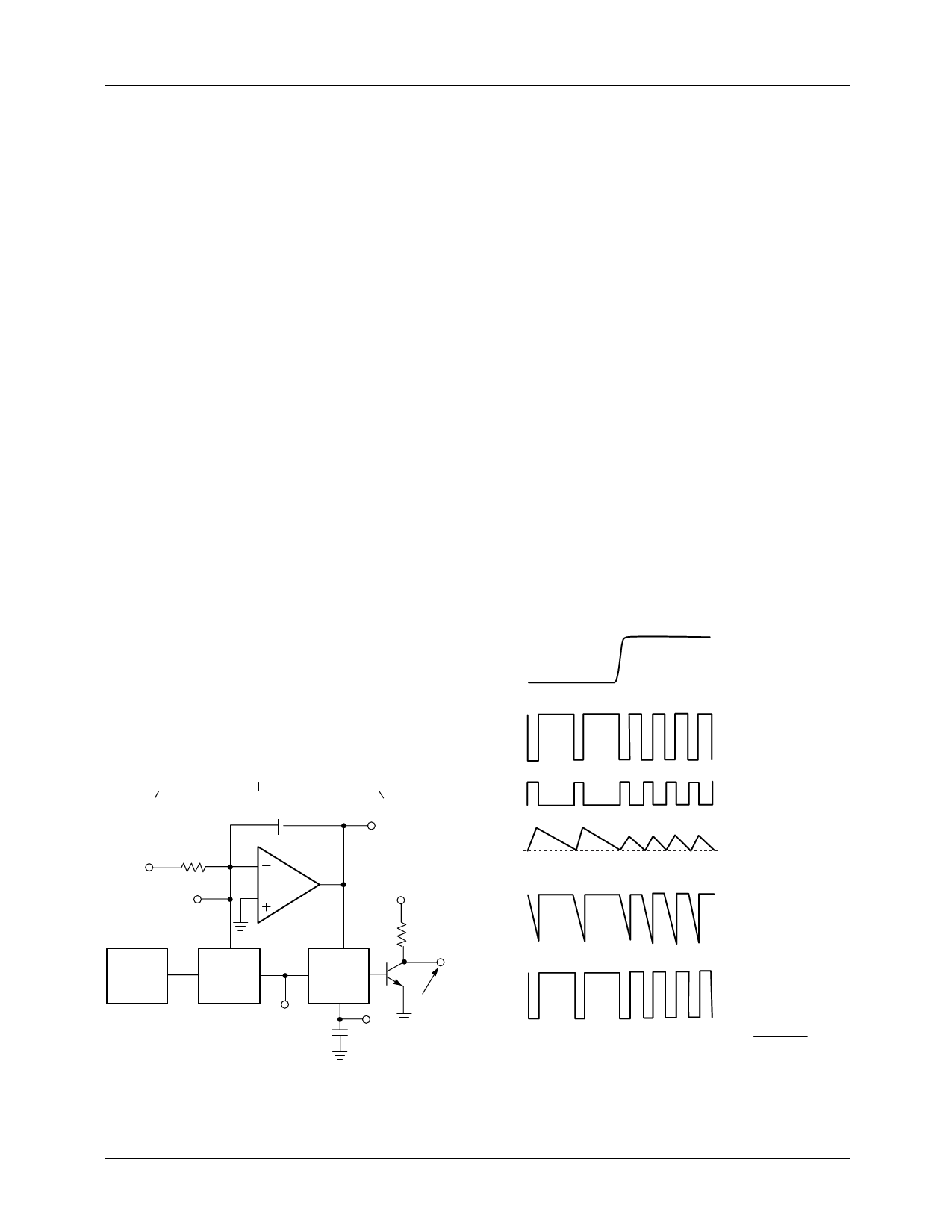
Integrator
CI
VIN
0 to 10V
R IN
A
I oUT
Voltage
Reference
7.3V
Switched
Current
Source
B
Co
(Timing)
C
+VS
Trigger
One
Shot
D
Ext
Load
E
Open
Collector
Output
4153-07
Figure 4. Voltage-to-Frequency Block Diagram
The scale factor K (the number of pulses per second or a
specified VIN), is adjusted by changing either RIN and there-
fore IIN, or by changing the amount of charge in each IOUT
pulse. Since the magnitude of IOUT is fixed at 1 milliamp, the
way to change the amount of charge is by adjusting the one-
shot duration set by CO (IOUT may be adjusted by changing
VREF). The accuracy of the relationship between VIN and
FOUT is affected by three major sources of error: temperature
drift, nonlinearity and offset.
The total temperature drift is the sum of the individual drift
of the components that make up the system. The greatest
source of drift in a typical application is in the timing
capacitor, CO. Low temperature coefficient capacitors, such
as silver mica and polystyrene, should be measured for drift
using a capacitance meter. Experimentation has shown that
the lowest tempco’s are achieved by wiring a parallel capaci-
tor composed of 70% silver mica and 30% polystyrene.
The reference on the chip can be replaced by an external
reference with much tighter drift specifications, such as an
LM199. The 199’s 6.9V output is close to the 4153’s 7.3V
output, and has less than 10 ppm/°C drift.
Nonlinearity is primarily caused by changes in the
precise amount of charge in each IOUT pulse. As frequency
increases, internal stray capacitances and switching
problems change the width and amplitude of the IOUT pulses,
causing a nonlinear relationship between VIN and FOUT.
+10V
VIN
+5V
0
A
-I OUT
B
C
Switched Current
Source Output
-1.0 mA
Switched Current Source
Logic (Internal)
Integrator Output
VTRIGGER ~~ +1.3V
-0.65V
D
One Shot Timing (CO)
T = 1.5 x 10 4 CO
-4.1V
-VS
E
Logic Output
-0.2V
V IN
F O = 2V REFR IN CO
4153-08
Figure 5. Voltage-to-Frequency Timing Waveforms
9
Share Link: 