RC4153 Ver la hoja de datos (PDF) - Fairchild Semiconductor
Número de pieza
componentes Descripción
Fabricante
RC4153 Datasheet PDF : 16 Pages
| |||
PRODUCT SPECIFICATION
RC4153
For this reason, the scale factor you choose should be below
1 KHz/V or as low as the acquisition time of your system
will allow.
Nonlinearity is also affected by the rate of CI to CO. Less
error can be achieved by increasing the value of CI, but this
affects response time and temperature drift. Optimum value
for CI and CO are shown In the tables in Figures 1, 2, and 3.
These values represent the best compromise of nonlinearity
and temperature drift. Polypropylene, mylar or polystyrene
capacitors should be used for CI.
The accuracy at low input voltages is limited by the offset
and VOS drift of the op amp. To improve this condition, an
offset adjust is provided.
Once your system is running, it may be calibrated as follows:
apply a measured full scale input voltage and adjust RIN until
the scale factor is correct. For precise applications, trimming
by soldering metal film resistors in parallel is recommended
instead of trimpots, which have bad tempco’s and are easily
taken out of adjustment by mechanical shock. After the scale
factor is calibrated, apply a known small input voltage
(approximately 10 mV) and adjust the op amp offset until the
output frequency equals the input multiplied by the scale
factor.
The output E consists of a series of negative going pulses
with a pulse width equal to the one-shot time. The open
collector pull-up resistor may be connected to a different
supply (such as 5V for TTL) as long a it does not exceed the
value of +VS applied to pin 10. The load current should be
kept below 10 mA in order to minimize strain on the device.
Pins 2 and 8 must be grounded in all applications, even if the
open collector transistor is not used.
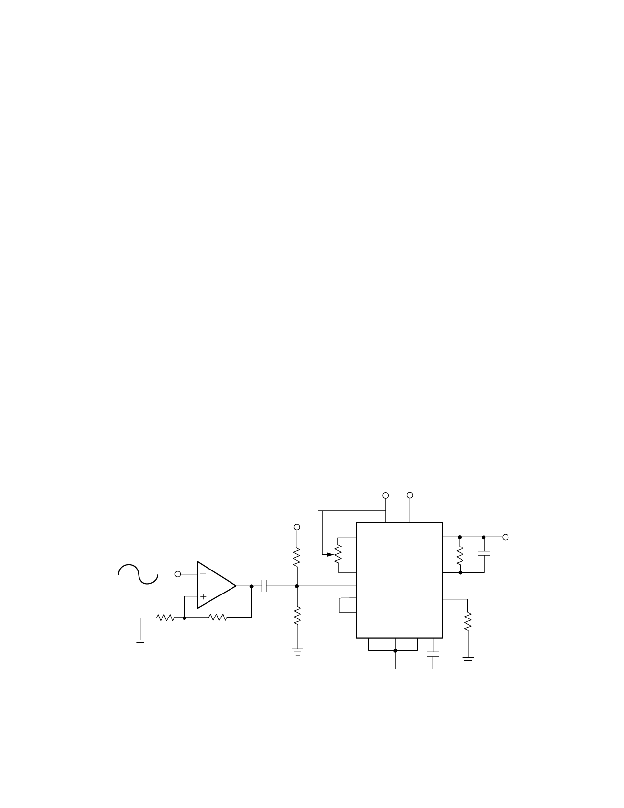
Figure 6 shows the complete circuit for a precision
frequency-to-voltage converter. The circuit converts an
input frequency to a proportional voltage by integrating the
switched current source output. As the input frequency
increases, the number of IOUT pulses delivered to the integra-
tor increases, thus increasing the average output voltage.
Depending on the time constant of the integrator, there will
be some ripple on the output. The output may be further
filtered, but this will reduce the response time. A second
order filter will decrease ripple and improve response time.
The input waveform must meet three conditions for proper
frequency-to-voltage operation. First, it must have sufficient
amplitude and offset to swing above and below the 1.3V
trigger threshold (See Figure 6 for an example of AC
coupling and offset bias.) Second, it must be a fast slewing
waveform having a quick rise time. A comparator may be
used to square it up. Finally, the input pulse width must not
exceed the one-shot time, in order to avoid retriggering the
one-shot (AC couple the Input).
Capacitive coupling between the trigger input and the timing
capacitor pin may occur if the input waveform is a square-
wave or the input has a short period. This can cause gross
nonlinearity due to changes in the one-shot timing waveform
(See Figure 7). This problem can be avoided by keeping the
value of CO small, and thereby keeping the timing period
less than the input waveform period.
-15V +15V
+VS
RA
F IN
CA
RB
100 W
100K
Comparator with
Hysteresis
Input
Coupling
1
13
-VS
VOS2
10
+VS
VOUT
4
14 VOS1
7
Trig
3
VREF
5 IIN
4153
RI
-In
12
+In 11
RI
GND2 GND1 FOUT CO
2
8 96
CO
Figure 6. Frequency-to-Voltage Precision Converter
VOUT+
CI
4153-09
10
Share Link: 