RT9199GSP Ver la hoja de datos (PDF) - Richtek Technology
Número de pieza
componentes Descripción
Fabricante
RT9199GSP Datasheet PDF : 13 Pages
| |||
RT9199
Functional Pin Description
VIN
Input voltage which supplies current to the output pin. Connect this pin to a well-decoupled supply voltage. To prevent the
input rail from dropping during large load transient, a large, low ESR capacitor is recommended to use. The capacitor
should be placed as close as possible to the VIN pin.
GND (Exposed Pad)
Common Ground. The exposed pad must be soldered to a large PCB and connected to GND for maximum power
dissipation.
VCNTL
VCNTL supplies the internal control circuitry and provides the drive voltage. The driving capability of output current is
proportioned to the VCNTL. Connect this pin to 5V bias supply to handle large output current with at least 1μF capacitor
from this pin to GND. An important note is that VIN should be kept lower or equal to VCNTL.
REFEN
Reference voltage input and active low shutdown control pin. Two resistors dividing down the VIN voltage on the pin to
create the regulated output voltage. Pulling the pin to ground turns off the device by an open-drain, such as 2N7002,
signal N-MOSFET.
VOUT
Regulator output. VOUT is regulated to REFEN voltage that is used to terminate the bus resistors. It is capable of sinking
and sourcing current while regulating the output rail. To maintain adequate large signal transient response, typical value
of 1000μF Al electrolytic capacitor with 10μF ceramic capacitors are recommended to reduce the effects of current
transients on VOUT.
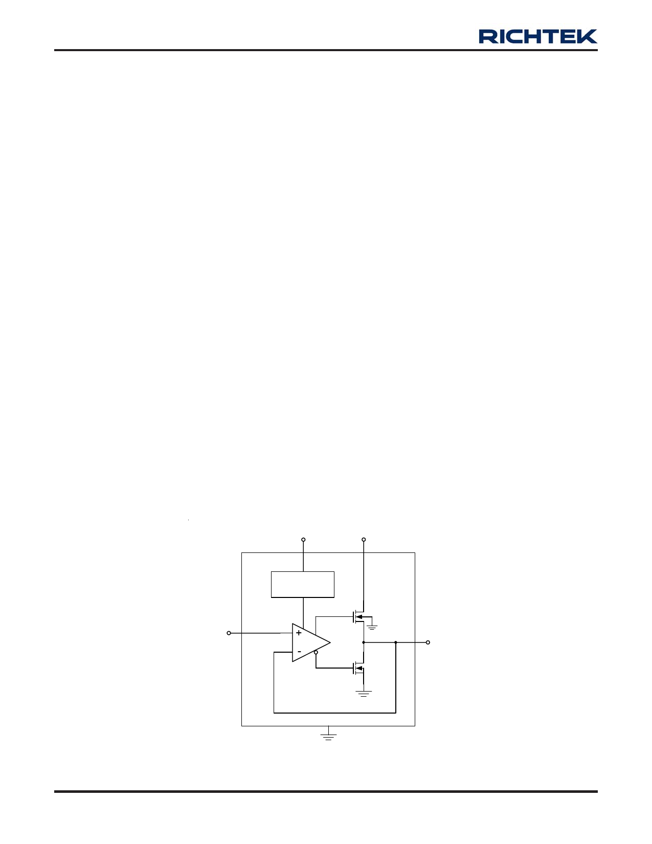
Function Block Diagram
VCNTL
VIN
REFEN
Current Limit
Thermal Protection
EA
VOUT
www.richtek.com
4
GND
DS9199-07 September 2007
Share Link: 