NLV14538BDWG Ver la hoja de datos (PDF) - ON Semiconductor
Número de pieza
componentes Descripción
Fabricante
NLV14538BDWG Datasheet PDF : 13 Pages
| |||
MC14538B
TRIGGER OPERATION
The block diagram of the MC14538B is shown in
Figure 1, with circuit operation following.
As shown in Figure 1 and 10, before an input trigger
occurs, the monostable is in the quiescent state with the Q
output low, and the timing capacitor CX completely charged
to VDD. When the trigger input A goes from VSS to VDD
(while inputs B and Reset are held to VDD) a valid trigger is
recognized, which turns on comparator C1 and N−channel
transistor N1 ➀. At the same time the output latch is set. With
transistor N1 on, the capacitor CX rapidly discharges toward
VSS until Vref1 is reached. At this point the output of
comparator C1 changes state and transistor N1 turns off.
Comparator C1 then turns off while at the same time
comparator C2 turns on. With transistor N1 off, the capacitor
CX begins to charge through the timing resistor, RX, toward
VDD. When the voltage across CX equals Vref 2, comparator
C2 changes state, causing the output latch to reset (Q goes
low) while at the same time disabling comparator C2 ➁. This
ends at the timing cycle with the monostable in the quiescent
state, waiting for the next trigger.
In the quiescent state, CX is fully charged to VDD causing
the current through resistor RX to be zero. Both comparators
are “off” with total device current due only to reverse
junction leakages. An added feature of the MC14538B is
that the output latch is set via the input trigger without regard
to the capacitor voltage. Thus, propagation delay from
trigger to Q is independent of the value of CX, RX, or the duty
cycle of the input waveform.
RETRIGGER OPERATION
The MC14538B is retriggered if a valid trigger occurs ➂
followed by another valid trigger ➃ before the Q output has
returned to the quiescent (zero) state. Any retrigger, after the
timing node voltage at pin 2 or 14 has begun to rise from
Vref 1, but has not yet reached Vref 2, will cause an increase
in output pulse width T. When a valid retrigger is initiated
➃, the voltage at CX/RX will again drop to Vref 1 before
progressing along the RC charging curve toward VDD. The
Q output will remain high until time T, after the last valid
retrigger.
RESET OPERATION
The MC14538B may be reset during the generation of the
output pulse. In the reset mode of operation, an input pulse
on Reset sets the reset latch and causes the capacitor to be
fast charged to VDD by turning on transistor P1 ➄. When the
voltage on the capacitor reaches Vref 2, the reset latch will
clear, and will then be ready to accept another pulse. It the
Reset input is held low, any trigger inputs that occur will be
inhibited and the Q and Q outputs of the output latch will not
change. Since the Q output is reset when an input low level
is detected on the Reset input, the output pulse T can be made
significantly shorter than the minimum pulse width
specification.
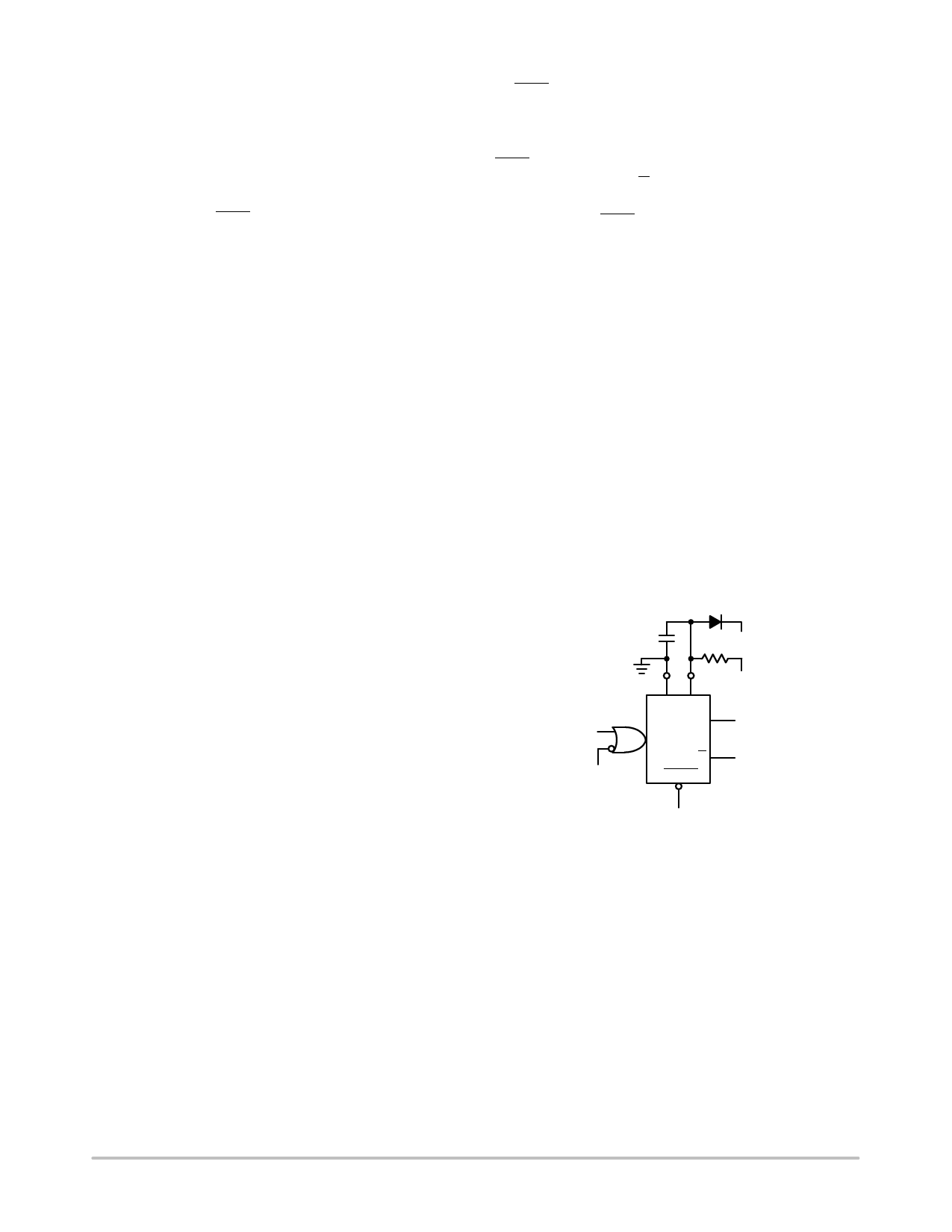
POWER−DOWN CONSIDERATIONS
Large capacitance values can cause problems due to the
large amount of energy stored. When a system containing
the MC14538B is powered down, the capacitor voltage may
discharge from VDD through the standard protection diodes
at pin 2 or 14. Current through the protection diodes should
be limited to 10 mA and therefore the discharge time of the
VDD supply must not be faster than (VDD). (C) / (10 mA).
For example, if VDD = 10 V and CX = 10 mF, the VDD supply
should discharge no faster than (10 V) x (10 mF) / (10 mA)
= 10 ms. This is normally not a problem since power
supplies are heavily filtered and cannot discharge at this rate.
When a more rapid decrease of VDD to zero volts occurs,
the MC14538B can sustain damage. To avoid this possibility
use an external clamping diode, DX, connected as shown in
Fig. 11.
Cx
VSS
Dx
Rx VDD
VDD
Q
Q
RESET
Figure 11. Use of a Diode to Limit
Power Down Current Surge
http://onsemi.com
8
Share Link: 