AD645 Ver la hoja de datos (PDF) - Analog Devices
Número de pieza
componentes Descripción
Fabricante
AD645 Datasheet PDF : 8 Pages
| |||
AD645
ABSOLUTE MAXIMUM RATINGS1
Supply Voltage . . . . . . . . . . . . . . . . . . . . . . . . . . . . . . . . ± 18 V
Internal Power Dissipation2 (@ TA = +25°C)
8-Pin Header Package . . . . . . . . . . . . . . . . . . . . . . 500 mW
AD645A/B/C . . . . . . . . . . . . . . . . . . . . . . . –40°C to +85°C
AD645S . . . . . . . . . . . . . . . . . . . . . . . . . . –55°C to +125°C
Lead Temperature Range
(Soldering 60 sec) . . . . . . . . . . . . . . . . . . . . . . . . . . . +300°C
8-Pin Mini-DIP Package . . . . . . . . . . . . . . . . . . . . 750 mW
Input Voltage . . . . . . . . . . . . . . . . . . . . . . . . . . . . . . . . . . . ± VS
Output Short Circuit Duration . . . . . . . . . . . . . . . . Indefinite
NOTES
1Stresses above those listed under “Absolute Maximum Ratings” may cause
permanent damage to the device. This is a stress rating only and functional
Differential Input Voltage . . . . . . . . . . . . . . . . . . +VS and –VS
Storage Temperature Range (H) . . . . . . . . . –65°C to +150°C
Storage Temperature Range (N) . . . . . . . . . –65°C to +125°C
Operating Temperature Range
AD645J/K . . . . . . . . . . . . . . . . . . . . . . . . . . . 0°C to +70°C
CAUTION
operation of the device at these or any other conditions above those indicated
in the operational section of this specification is not implied. Exposure to
absolute maximum rating conditions for extended periods may affect device
reliability.
2Thermal Characteristics:
8-Pin Plastic Mini-DIP Package: θJA = 100°C/Watt
8-Pin Header Package: θJA = 200°C/Watt
ESD (electrostatic discharge) sensitive device. Electrostatic charges as high as 4000 V readily
accumulate on the human body and test equipment and can discharge without detection.
WARNING!
Although the AD645 features proprietary ESD protection circuitry, permanent damage may
occur on devices subjected to high energy electrostatic discharges. Therefore, proper ESD
precautions are recommended to avoid performance degradation or loss of functionality.
ESD SENSITIVE DEVICE
ORDERING GUIDE
Model1
Temperature Range Package Option2
AD645JN
AD645KN
AD645AH
AD645BH
AD645CH
AD645SH/883B
0°C to +70°C
0°C to +70°C
– 40°C to +85°C
– 40°C to +85°C
– 40°C to +85°C
– 55°C to +125°C
N-8
N-8
H-08A
H-08A
H-08A
H-08A
NOTES
1Chips are also available.
2N = Plastic Mini-DIP; H = Metal Can.
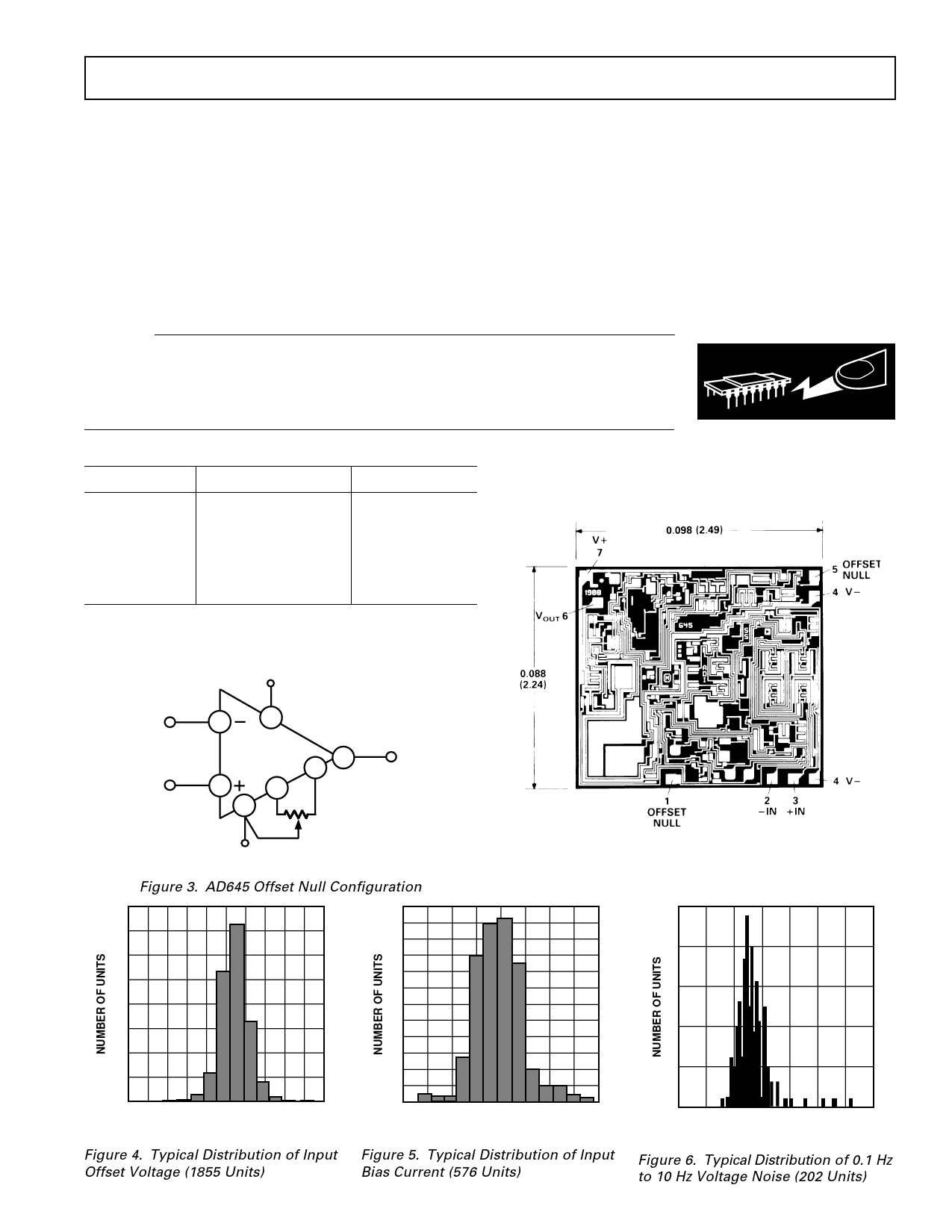
+VS
METALIZATION PHOTOGRAPH
Dimensions shown in inches and (mm).
Contact factory for latest dimensions.
2
7
AD645
6
5
3
4
1
10k
VOS ADJUST
–VS
Figure 3. AD645 Offset Null Configuration
800
700
600
500
400
300
200
100
0
–1.0 –0.8 –0.6 –0.4 –0.2 0.0 0.2 0.4 0.6 0.8 1.0
INPUT OFFSET VOLTAGE – mV
120
110
100
90
80
70
60
50
40
30
20
10
0
0.0 0.5 1.0 1.5 2.0 2.5 3.0 3.5 4.0
INPUT BIAS CURRENT – pA
Figure 4. Typical Distribution of Input
Offset Voltage (1855 Units)
REV. B
Figure 5. Typical Distribution of Input
Bias Current (576 Units)
–3–
25
20
15
10
5
0
0.4 0.6 0.8 1.0 1.2 1.4 1.6 1.8
INPUT VOLTAGE NOISE – µV p-p
Figure 6. Typical Distribution of 0.1 Hz
to 10 Hz Voltage Noise (202 Units)
Share Link: 