AT17LV256-10NC Ver la hoja de datos (PDF) - Atmel Corporation
Número de pieza
componentes Descripción
Fabricante
AT17LV256-10NC Datasheet PDF : 14 Pages
| |||
AT17C/LV65/128/256
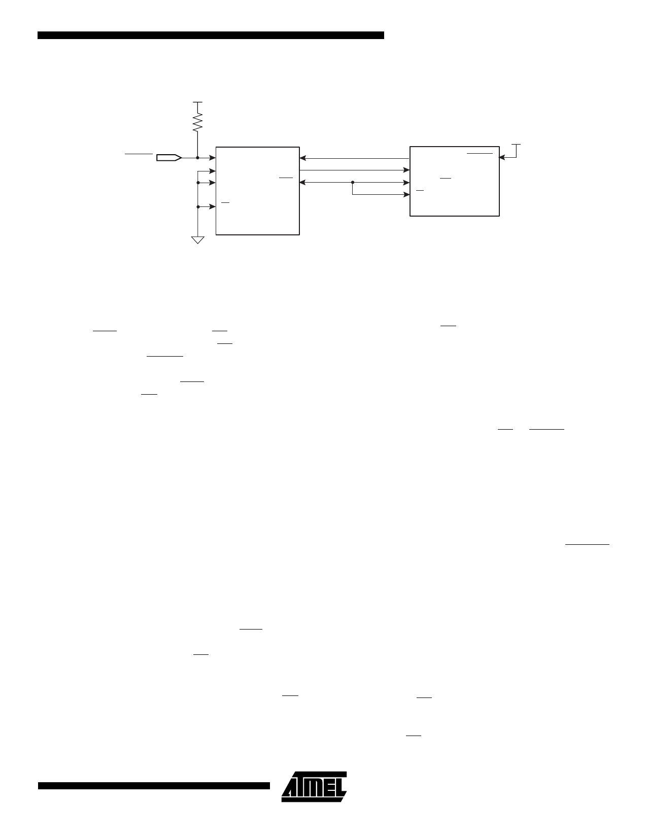
Figure 1. Condition 1 Connection
VCC
REBOOT
AT60xx
M2
D0
M1
CCLK
M0
CON
CS
AT17C65/128/256
AT17LV65/128/256
DATA
CLK
RESET/OE
CE
SER_EN
VCC
GND
Notes: 1. 4.7 kΩ resistors used unless otherwise specified.
2. Reset polarity of EEPROM must be set active High.
Condition 2
The FPGA CON pin drives only the CE input of the AT17
Series Configurator, while the RESET/OE input is driven by
an input to the FPGA RESET input pin. This connection
works under all normal circumstances, even when the user
aborts a configuration before CON has gone High. A Low
level on the RESET/OE(1) input – during FPGA reset –
clears the Configurator’s internal address pointer, so that
the reconfiguration starts at the beginning.
Note: 1. For this condition, the reset polarity of the EEPROM
must be set active Low.
The AT17 Series Configurator does not require an
inverter for either condition since the RESET polarity is
programmable.
If the address counters are not to be reset upon comple-
tion, then the RESET/OE input can be tied to its inactive
(default Low) level.
Note: 1. A single AT17C/LV65 may be used at the end of a
cascade chain.
AT17 Series Reset Polarity
The AT17 Series Configurator allows the user to program
the reset polarity as either RESET/OE or RESET/OE. This
feature is supported by industry-standard programmer
algorithms. For more details on programming the
EEPROM’s reset polarity, please reference the “Program-
ming Specification for Atmel’s FPGA Configuration
EEPROMs” application note.
Cascading Serial Configuration
EEPROMs
(AT17C/LV128 and AT17C/LV256 only)(1)
For multiple FPGAs configured as a daisy-chain, or for
future FPGAs requiring larger configuration memories,
cascaded Configurators provide additional memory.
After the last bit from the first Configurator is read, the next
clock signal to the Configurator asserts its CEO output low
and disables its DATA line driver. The second Configurator
recognizes the Low level on its CE input and enables its
DATA output.
After configuration is complete, the address counters of all
cascaded Configurators are reset if the RESET/OE on
each Configurator is driven to its active (default High) level.
Programming Mode
The programming mode is entered by bringing SER_EN
Low. In this mode the chip can be programmed by the
2-wire serial bus. The programming is done at VCC supply
only. Programming super voltages are generated inside the
chip. See the “Programming Specification for Atmel’s
FPGA Configuration EEPROMs” application note for
further information. The AT17C parts are read/write at 5V
nominal. The AT17LV parts are read/write at 3.3V nominal.
Standby Mode
The AT17C/LV65/128/256 enters a low-power standby
mode whenever CE is asserted High. In this mode, the
Configurator consumes less than 75 µA of current at 5.0V.
The output remains in a high impedance state regardless of
the state of the OE input.
3
Share Link: 