AS1361 Ver la hoja de datos (PDF) - austriamicrosystems AG
Número de pieza
componentes Descripción
Fabricante
AS1361
austriamicrosystems AG

AS1361 Datasheet PDF : 15 Pages
| |||
AS1361/AS1362
Datasheet - Detailed Description
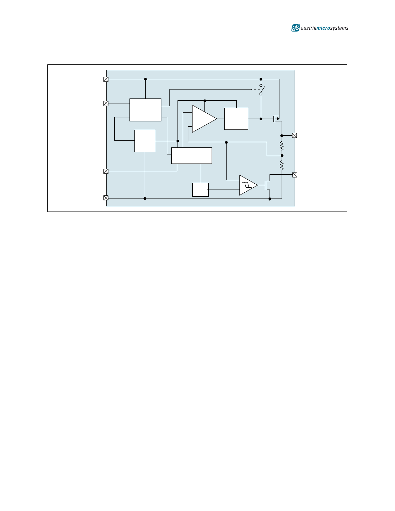
Figure 18. AS1361/AS1362 - Block Diagram
AS1361/AS1362
IN
SHDNN
BYPASS
GND
Shutdown and
Power-Down
Control
Thermal
Sensor
-
Error
Amp
+
1.25 Reference
and Noise Bypass
MOS
Driver w/
ILIMIT
–
95%
+
OUT
POK
Power-OK
The power-ok circuitry is built around an N-channel MOSFET. The circuitry monitors the output voltage and if the volt-
age goes out of regulation (e.g. during dropout, current limit, or thermal shutdown) pin POK goes low.
The power-OK feature is not active during shutdown and provides a power-on-reset (POR) function that can operate
down to VIN = 1V. A capacitor to GND may be added to generate a POR delay.
To obtain a logic-level output, connect a pull-up resistor from pin POK to pin OUT. Larger values for this resistor will
help minimize current consumption; a 100kΩ resistor is perfect for most applications (see Figure 1 on page 1).
Current Limit
The AS1361/AS1362 include a current limiting circuitry to monitor and control the P-channel MOSFET pass transis-
tor’s gate voltage, thus limiting the device output current to 270mA (AS1361) and 510mA (AS1362).
Note: See Table 4 on page 4 for the recommended min and max current limits. The output can be shorted to ground
indefinitely without causing damage to the device.
Thermal Protection
Integrated thermal protection circuitry limits total power dissipation in the AS1361/AS1362. When the junction temper-
ature (TJ) exceeds +160ºC, the thermal sensor signals the shutdown logic, turning off the P-channel MOSFET pass
transistor and allowing the device to cool down. The thermal sensor turns the pass transistor on again after the
device’s junction temperature drops by 10ºC, resulting in a pulsed output during continuous thermal-overload condi-
tions.
Note: Thermal protection is designed to protect the devices in the event of fault conditions. For continuous operation,
do not exceed the absolute maximum junction temperature rating of +150ºC.
Operating Region and Power Dissipation
The AS1361/AS1362 maximum power dissipation is dependant on the thermal resistance of the case and PCB, the
temperature difference between the die junction and TAMB, and airflow rate.
Power dissipation across the device is calculated as:
PD = IOUT (VIN - VOUT)
(EQ 1)
www.austriamicrosystems.com
Revision 1.03
10 - 15
Share Link: