HV5222 Ver la hoja de datos (PDF) - Supertex Inc
Número de pieza
componentes Descripción
Fabricante
HV5222 Datasheet PDF : 10 Pages
| |||
HV5222
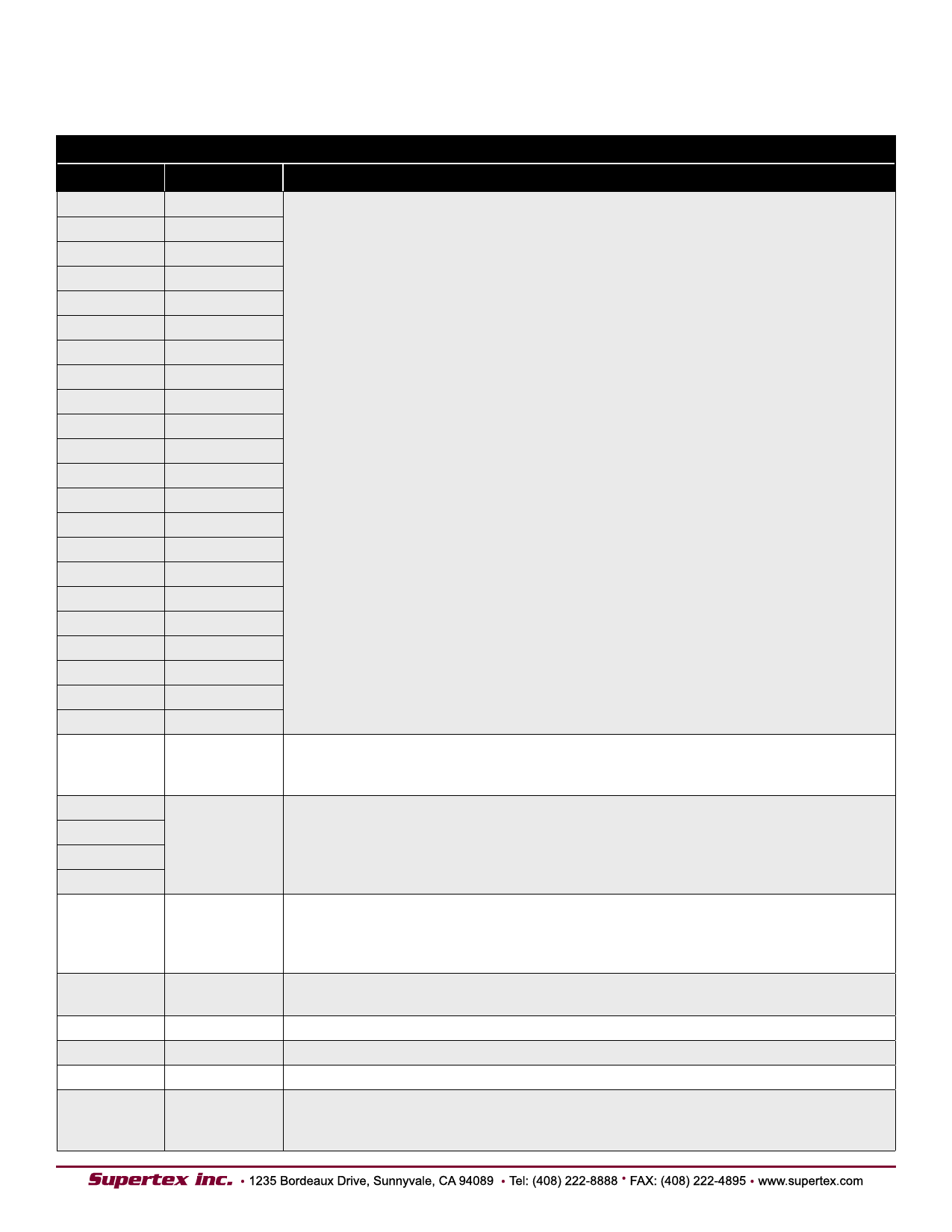
44-Lead PQFP Pin Assignment (PG)
HV5222PG
Pin
Function Description
1
HVOUT22
2
HVOUT21
3
HVOUT20
4
HVOUT19
5
HVOUT18
6
HVOUT17
7
HVOUT16
8
HVOUT15
9
HVOUT14
10
HVOUT13
11
HVOUT12
High voltage outputs.
12
HVOUT11
13
HVOUT10
14
HVOUT9
15
HVOUT8
16
HVOUT7
17
HVOUT6
18
HVOUT5
19
HVOUT4
20
HVOUT3
21
HVOUT2
22
HVOUT1
Serial data output
23
DATA OUT
Data output for cascading to the data input of the next device.
24
25
N/C
No connect.
26
27
Output enable input.
28
OE
When OE is LOW, all HV outputs are forced into a LOW state, regardless of data in
each channel. When OE is HIGH, all HV outputs reflect data latched.
29
CLK
Data shift register clock.
Input are shifted into the shift register on the positive edge of the clock.
30
GND
Logic and high voltage ground.
31
VDD
Low voltage logic power rail.
32
STR
Strobe.
Serial data input
33
DATA IN
Data needs to be present before each rising edge of the clock.
5
Share Link: 