RF105 Ver la hoja de datos (PDF) - Conexant Systems
Número de pieza
componentes Descripción
Fabricante
RF105 Datasheet PDF : 12 Pages
| |||
RF105
Synthesizer Programming ________________________
The synthesizer is programmed with a half-duplex 3-wire
serial interface. The three signals are DATA, CLK, and
STROBE. Each rising edge of the CLK signal shifts one bit
of the data into the shift register and control register. When
the STROBE input is toggled from low to high, the data
latched in the shift register is transferred to the
programmable counter. Six bits are shifted into the
synthesizer for programming. The data format is as
follows:
MSB
LSB
S6
S5
S4
S3
S2
S1
The timing relationship is shown in Figure 6. The values of
the programming bits, S1 to S6, for the programmable
counter are defined in Table 1.
Channel Selection
Using a 9.6 MHz reference frequency, the Phase Locked
Loop (PLL) synthesizer can generate frequencies from
903 MHz (Channel 1) to 927 MHz (Channel 41) at a
channel spacing of 600 kHz. The LO frequency (FLO) is
calculated by the following equation:
FLO = (FREF/R) × [(M × N) + A]
where:
FREF is 9.6 MHz (reference oscillator)
R is 16 (reference divider)
M is 32/33 (prescaler)
N is 47 (fixed counter)
A is 1 to 41 (programmable counter)
900 MHz Digital Spread Spectrum Transceiver
Examples:
(9.6 MHz / 16) × (32 × 47 + 1) = 903 MHz
(9.6 MHz / 16) × (32 × 47 + 41) = 927 MHz
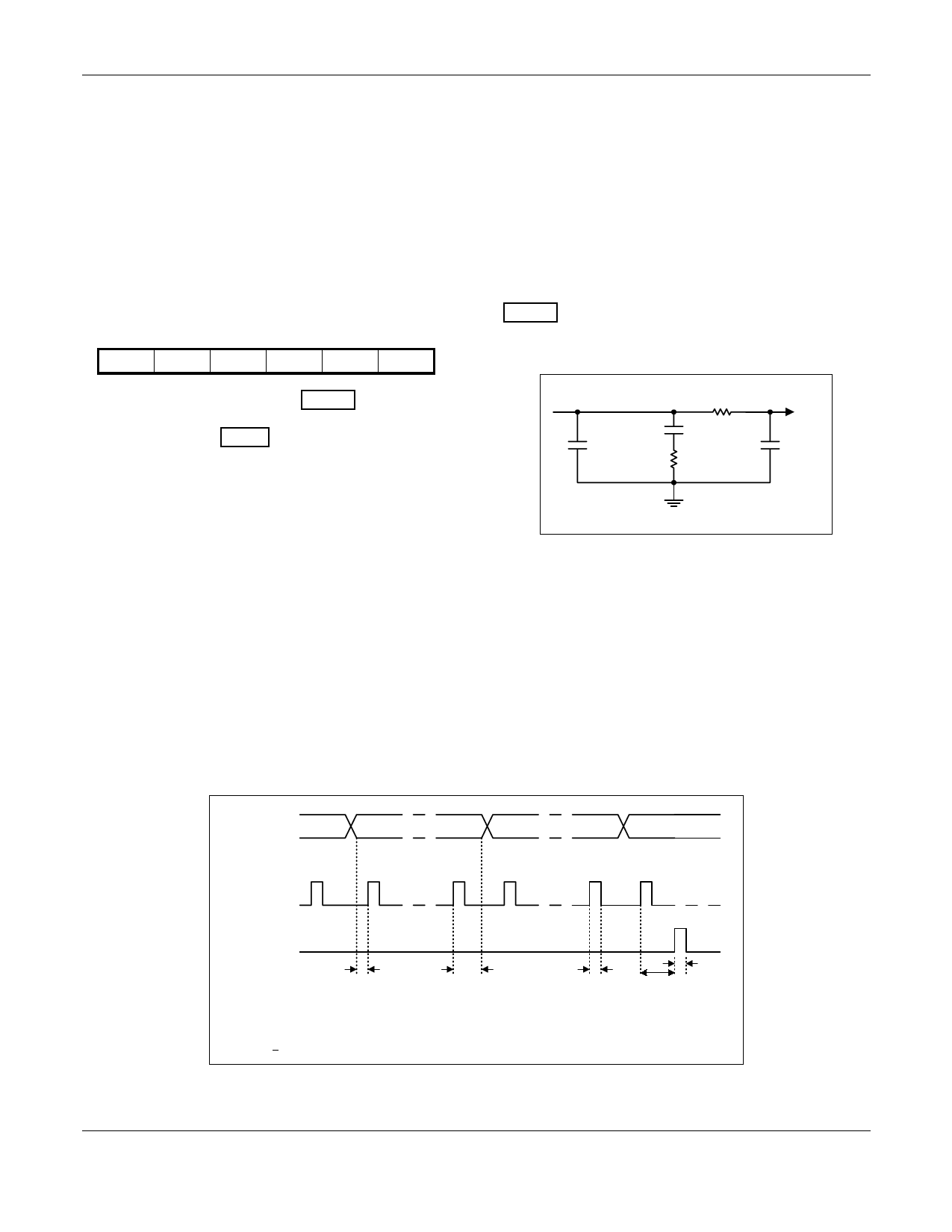
Synthesizer Loop Filter
The VCO for the synthesizer is designed on-chip with the
varactor referenced to VCC. Therefore, the loop filter
components will need to be tied to VCC4 (pin 39) instead
of ground. A typical loop filter design is shown below in
Figure 5. The loop bandwidth is approximately 5 kHz with a
nominal phase margin of 45 degrees.
CHPO
pin 43
0.01µF
390
pF
10kΩ
10kΩ
VCOTUNE
330
pF
Figure 5. Loop Filter
DATA MSB
LSB
CLK
STROBE
t1 =Data setup time
t1
t2
t3
t2 =Data hold time
t3 =Clock pulse-width
t4 =STROBE enable pulse-width
t5 =STROBE setup time to the rising edge of the last clock
t1 to t5 > 1µs each.
Figure 6. Timing Diagram
t4
t5
4
Conexant
W117, Rev. B
Conexant Proprietary Information
September 28, 1999
Share Link: 