DS1204V Ver la hoja de datos (PDF) - Dallas Semiconductor -> Maxim Integrated
Número de pieza
componentes Descripción
Fabricante
DS1204V Datasheet PDF : 10 Pages
| |||
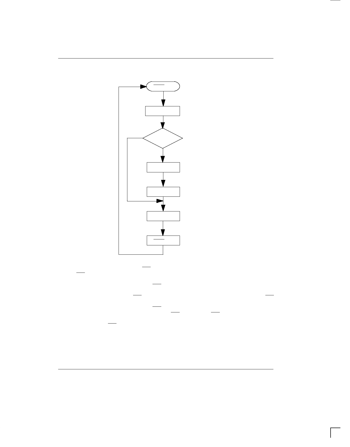
FLOW CHART - PROGRAM MODE Figure 6
RESET HIGH
WRITE COMMAND PROTOCOL
NO
MATCH
PROGRAM MODE
DS1204V
WRITE 64 BITS IDENTIFICATION
WRITE 64 BITS SECURITY MATCH
STOP
RESET LOW
OUTPUT IN HIGH Z
RESET AND CLOCK CONTROL
All data transfers are initiated by driving the RST input
high. The RST input serves three functions. First, it turns
on control logic, which allows access to the command
register for the command sequence. Second, the RST
signal provides a power source for the cycle to follow. To
meet this requirement, a drive source for RST of 2 mA @
3.5 volts is required. However, if the VCC pin is con-
nected to a 5-volt source within nominal limits, the RST
is not used as a source of power and input levels revert
to normal VIH and VIL inputs with a drive current require-
ment of 500 µA. Third, the RST signal provides a meth-
od of terminating data transfer.
A clock cycle is a sequence of a falling edge followed by
a rising edge. For data inputs, the data must be valid
during the rising edge of a clock cycle. Command bits
and data bits are input on the rising edge of the clock and
data bits are output on the falling edge of the clock. The
rising edge of the clock returns the DQ pin to a high im-
pedance state. All data transfer terminates if the RST
pin is low and the DQ pin goes to a high impedance
state. When data transfer to the key is terminated using
RST, the transition of RST must occur while the clock is
at a high level to avoid disturbing the last bit of data. Data
transfer is illustrated in Figure 8 for normal mode and
Figure 9 for program mode.
021798 5/10
Share Link: 