SP000219532 Ver la hoja de datos (PDF) - Infineon Technologies
Número de pieza
componentes Descripción
Fabricante
SP000219532
Infineon Technologies

SP000219532 Datasheet PDF : 16 Pages
| |||
PROFET® ITS711L1
Truth Table
Channel 1 and 2
Channel 3 and 4
(equivalent to channel 1 and 2)
Chip 1
Chip 2
IN1 IN2 OUT1 OUT2
IN3 IN4 OUT3 OUT4
ST1/2
ST3/4
BTS 711L1
Normal operation
L
L
L
L
H
L
H
L
H
H
H
L
H
L
H
H
H
H
H
H
Open load
Channel 1 (3) L
L
Z
L
H
Z
H
X
H
Channel 2 (4) L
L
L
L
H(L15))
H
H
X
L
Z
H(L15))
H
L
H
Z
H
X
H
X
H
L
Short circuit to Vbb
Channel 1 (3) L
L
H
L
H
H
H
X
H
Channel 2 (4) L
L
L
L
L16)
H
H
X
H(L17))
H
L16)
H
L
H
X
H
X
H
H
H
H(L17))
Overtemperature
both channel
L
L
L
L
H
X
H
L
L
L
H
X
L
L
L
Channel 1 (3) L
X
L
X
H
H
X
L
X
L
Channel 2 (4) X
L
X
L
H
X
H
X
L
L
Undervoltage/ Overvoltage
X
X
L
L
H
L = "Low" Level
X = don't care
Z = high impedance, potential depends on external circuit
H = "High" Level
Status signal valid after the time delay shown in the timing diagrams
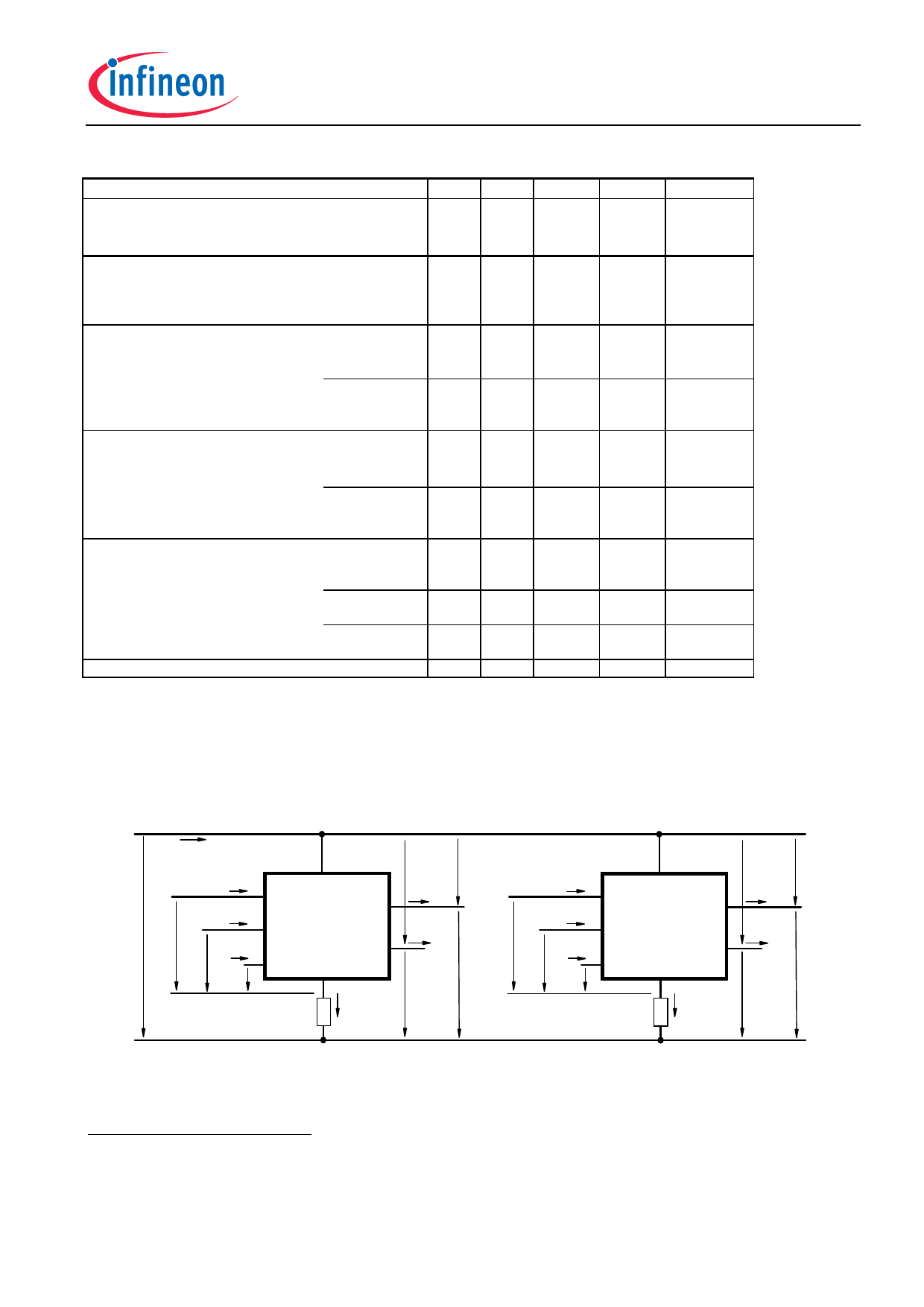
Parallel switching of channel 1 and 2 (also channel 3 and 4) is easily possible by connecting the inputs and
outputs in parallel (see truth table). If switching channel 1 to 4 in parallel, the status outputs ST1/2 and ST3/4
have to be configured as a 'Wired OR' function with a single pull-up resistor.
Terms
Ibb
Vbb
I IN1
3
IN1
Leadframe
Vbb
VON1
VON2
18 IL1
IIN2 5
IN2
I ST1/2
OUT1
PROFET
Chip 1 OUT2 17
IL2
VIN1 VIN2 VST1/2 4 ST1/2 GND1/2
2
VOUT1
IGND1/2 VOUT2
RGND1/2
Leadframe
VON3
I IN3
7
Vbb
IN3
VON4
14 IL3
IIN4 9
IN4
I ST3/4
OUT3
PROFET
Chip 2 OUT4 13
I L4
VIN3 VIN4 VST3/4 8 ST3/4 GND3/4
6
VOUT3
IGND3/4 VOUT4
RGND3/4
Leadframe (Vbb) is connected to pin 1,10,11,12,15,16,19,20
External RGND optional; two resistors RGND1/2 ,RGND3/4 = 150 Ω or a single resistor RGND = 75 Ω for
reverse battery protection up to the max. operating voltage.
15) With additional external pull up resistor
16) An external short of output to Vbb in the off state causes an internal current from output to ground. If RGND is
used, an offset voltage at the GND and ST pins will occur and the VST low signal may be errorious.
17) Low resistance to Vbb may be detected by no-load-detection
Infineon Technologies AG
7
2006-Mar-23
Share Link: