ACS103 Ver la hoja de datos (PDF) - Unspecified
Número de pieza
componentes Descripción
Fabricante
ACS103 Datasheet PDF : 10 Pages
| |||
twh
t
wl
TxCL and RxCL clock pulse widths
t
r
t
f
90 % 90 %
10 %
10 %
Digital Outputs rise and fall times
TxCL
RxCL
t
t
sut
ht
2
t
t
sur
hr
TxD
RxD
Transmit set-up and hold times
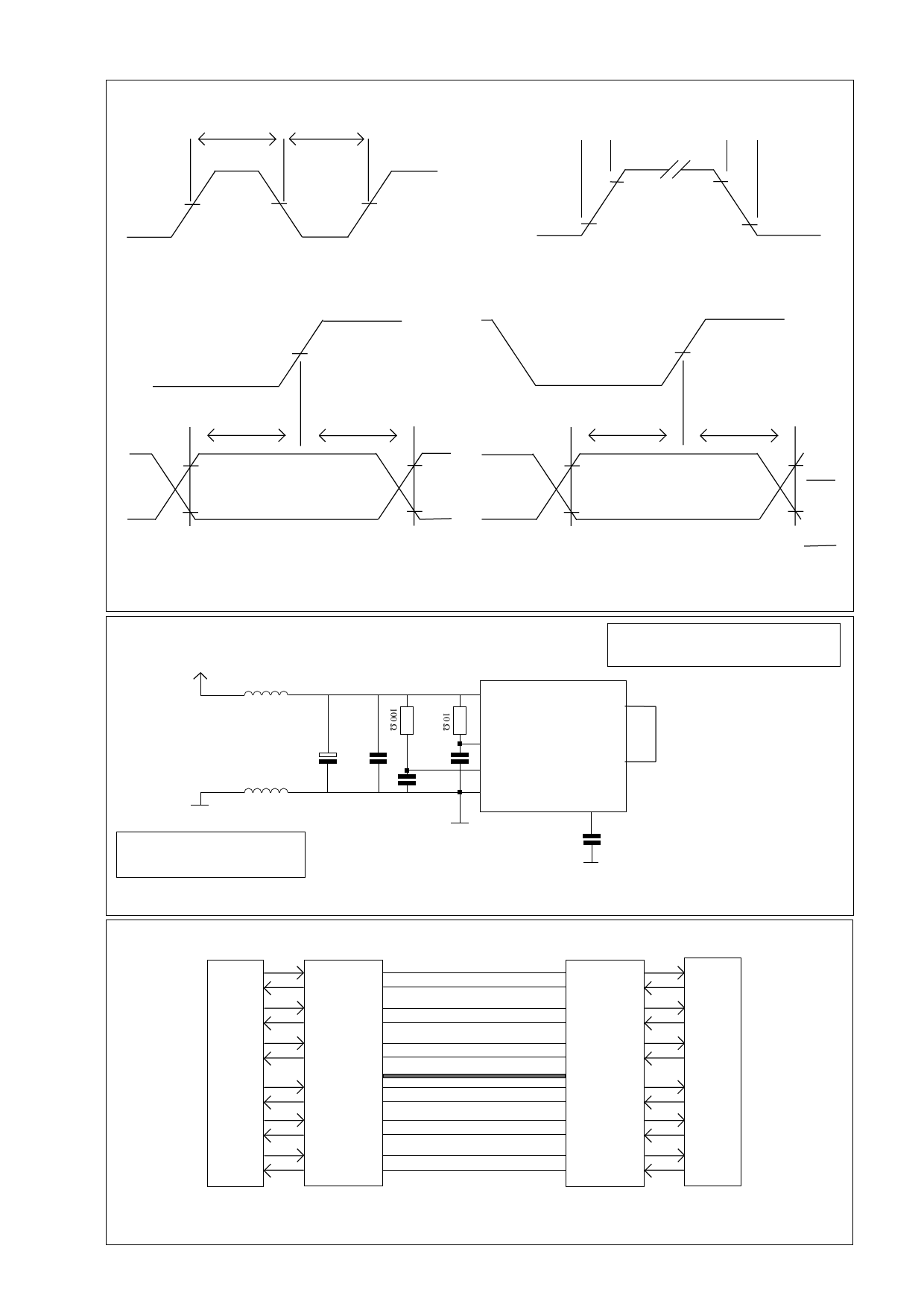
Figure 2. Timing diagrams
Receive set-up and hold times
VD+ pins are 13, 37, 38, 67 and 68.
V+
GND pins are 23, 35, 36, 47, 65 and 66.
+5V
47 µH
GND
47 µH
47µF
100 nF
100 nF
100 nF
VA+
CON1
VD+ ACS103
CON2
VG
GND
CNT
Pin 49 and Pin 54
should be connected together
All capacitors must be placed
very close to the ACS103.
GND
22 - 33 nF
GND
Figure 3. Recommended power supply layout
DTE
ACS103
TxD1
RxD1
RTS / XI1
CTS / XO1
TxD2
RxD2
DTR / XI2
DSR / XO2
TxD3
RxD3
XI3
XO3
Single Fiber Link
ACS103
RxD1
TXD1
CTS / XO1
RTS / XI1
RxD2
TxD2
DSR / XO2
DTR / XI2
RxD3
TxD3
XO3
XI3
DCE
Figure 4. 6 Full-duplex channels in data transmission mode
7
ACS103 Issue 2.03 May 1996.
Share Link: 