CXD2555 Ver la hoja de datos (PDF) - Intersil
Número de pieza
componentes Descripción
Fabricante
CXD2555 Datasheet PDF : 11 Pages
| |||
HI2555, CXD2555
Master Mode/Slave Mode
(Related Pins) MS, LRCK, BCK
When using the XCS2555Q in multiple units or in a pair with
DA converters such as the CXD2558M, one of these
CXD2555Qs should be in the master mode to serve as the
source of clocks LRCK and BCK. The other CXD2555Qs are
used in the slave mode, with their clocks LRCK and BCK
supplied by the master CXD2555Q.
TABLE 3.
MS
MODE
H
Master Mode
L
Slave Mode
LRCK AND BCK I/O
Output
Input
Crystal Oscillator Frequency Selection
(fS = 32kHz to 48kHz)
(Related Pins) XTLI, XTLO, XSLO, XSL1, XSL2, UNCLK,
XCLK
By setting a combination of XSLO and XSL1, with XSL2
fixed Low, the frequency of the external crystal oscillator
connected to XTLI and XTLO can be selected. In this case,
XCLK outputs a clock whose frequency is always 256 times
fS, and UCLK outputs a clock that is half the crystal oscillator
frequency.
When supplying the master clock fro some other external
source, not a crystal oscillator, use XTLI for this clock input
and leave XTLO open.
XSL2
L
L
L
L
XSL1
L
L
H
H
XSL0
L
H
L
H
TABLE 4.
CRYSTAL OSCILLATOR FREQUENCY
256fS
512fS
768fS
1024fS
XCLK
256fS
256fS
256fS
256fS
UCLK
128fS
256fS
384fS
512fS
OUTPUT
LRCK
INPUT
LRCK
H
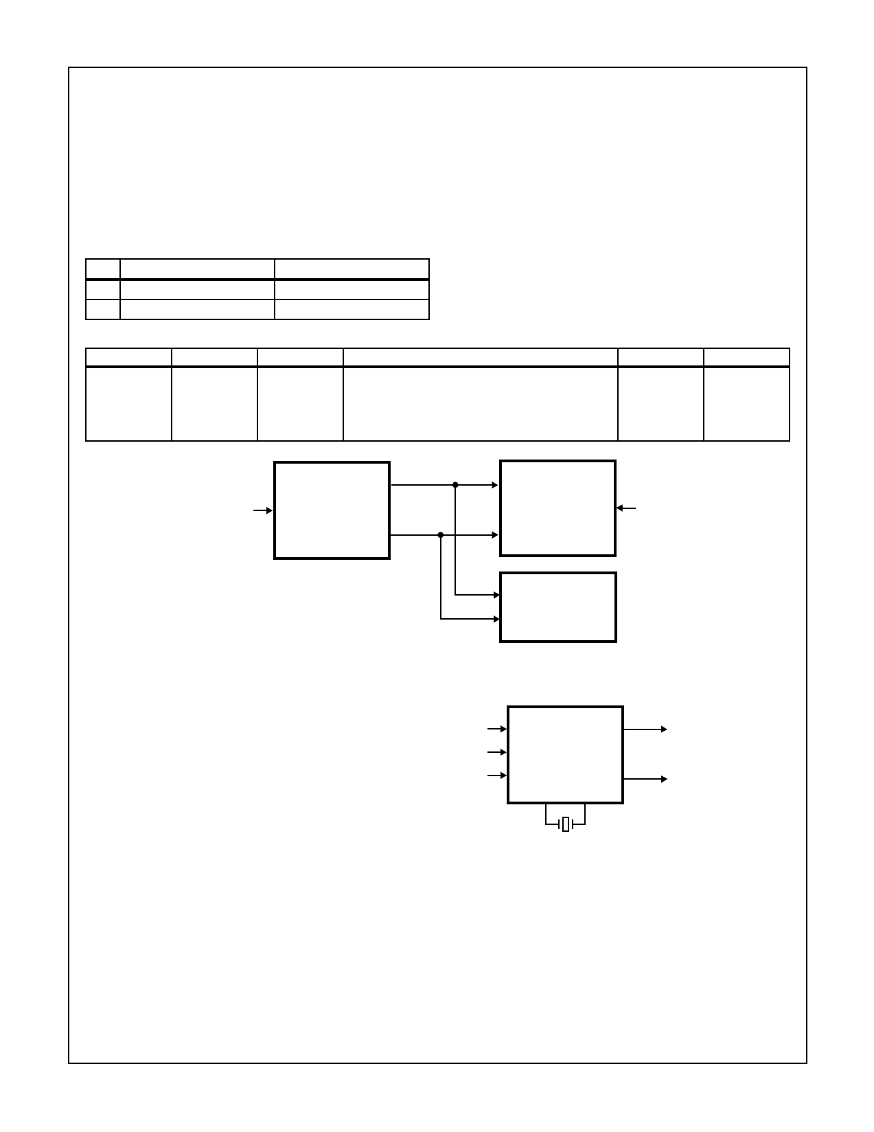
MS CXD2555Q
(MASTER MODE)
OUTPUT
INPUT
CXD2555Q MS
(SLAVE MODE)
L
BCK
BCK
INPUT
INPUT
LRCK
CXD2558M
BCK
FIGURE 37. CONNECTION EXAMPLE
Crystal Oscillator Frequency Selection
(fS = 8kHz to 24kHz)
(Related Pins) XTLI, XTLO, XSLO, XSL1, XSL2, UNCLK,
XCLK
With XSL2 fixed High, the device can be operated with low-
fS frequencies which may be 1/2 or 1/4 the normal fS
frequency. In this case, the frequency of the crystal oscillator
can be selected by setting a combination of XSL0 and XSL1
accordingly.
L
XSL2
UCLK
512fS
TO EXTERNAL IC,
SUCH AS DSP
H
XSL1 CXD2555Q
H
XSL0
XCLK
256fS
TO CXD2555Q IN
SLAVE MODE
XTL1 XTL0
1024fS
AD Converter Input Level
Given the constants shown in the Test Circuit on page 7, the
AD converter input level VIN (operational amplifier input IN)
is such that 4VP-P (1.4VRMS) is equivalent to the full-scale
output. Also, the large-amplitude inputs are possible by
varying the AD converter input resistance value (RIN). Use
the equation shown below to calculate this resistance value.
The AD converter generates full-scale outputs for inputs
equal to or greater than the values thus obtained.
RIN = 420 • VIN [RMS] - 1200 [Ω]
FIGURE 38. CONNECTION EXAMPLE
Example: When input level = 1.4VRMS (4VP-P)
RIN = 4200 • 1.4 - 1200 = 4680
→ 4700 [Ω]
4-308
Share Link: 