M62021 Ver la hoja de datos (PDF) - Renesas Electronics
Número de pieza
componentes Descripción
Fabricante
M62021 Datasheet PDF : 14 Pages
| |||
M62021L/P/FP
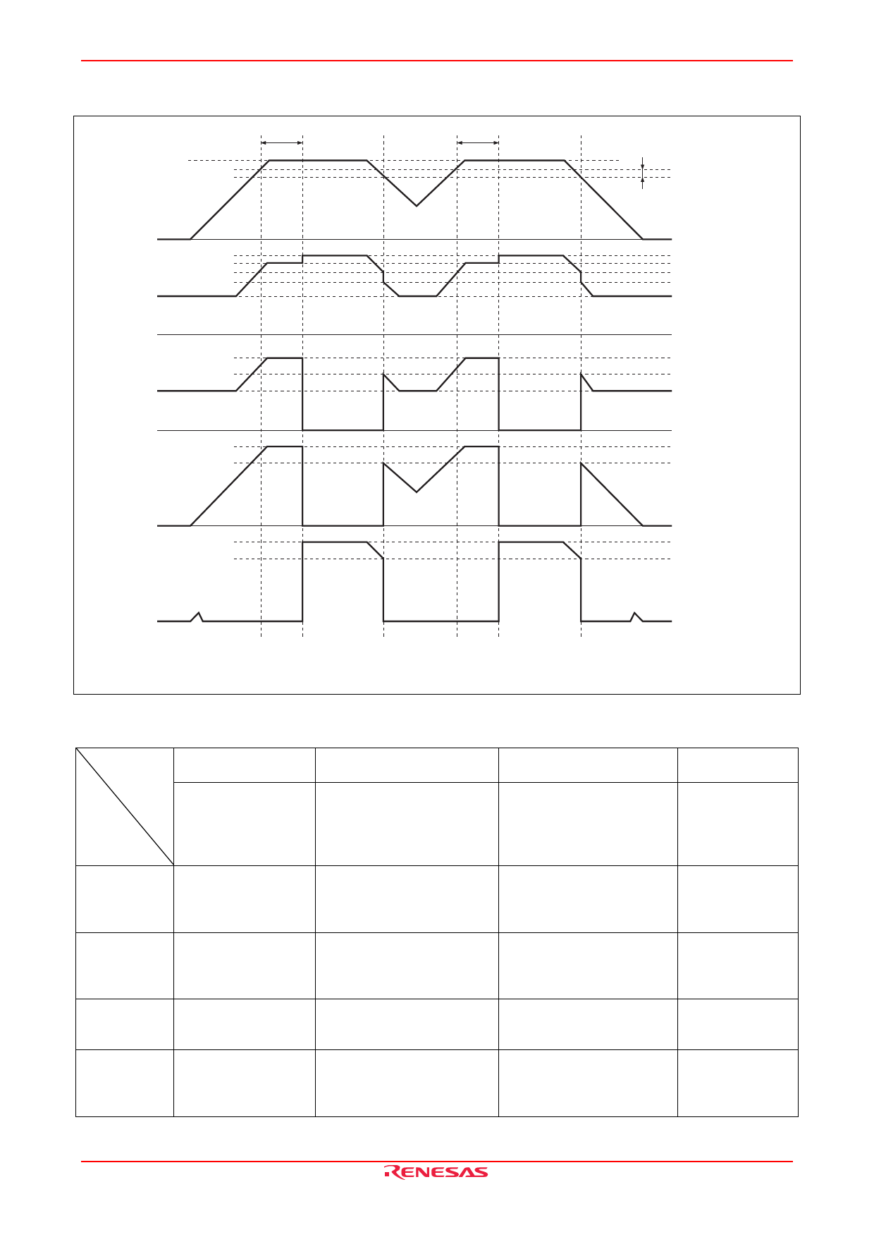
Timing Chart
tpd
5V
VIN
0V
VOUT
tpd
VSH
∆VS
VSL
V1
V2
V3
V4
V5
CS
RES
RES
V2
V4
V5
VOL(CS)
5V
VIN(VSL)
VOL(RES)
VOH(RES)
VIN(VSL)
V1 = VIN – VDROP
V2 = VIN – Q4VEB(Di)
V3 = VIN(VSL) – VDROP
VOL(RES)
V4 = VIN(VSL) – Q4VEB(Di)
V5 = VBAT – VF
Figure 6 Timing Chart
Input
Voltage
Output
Pin
VOUT
RES
RES
CS
In Normal Operation
Input voltage: 5V
With Q4 set to ON,
a voltage (VIN – VDROP)
is output
The output level is VOL
(RES) with a logic low
The output level is VOH
(RES) with a logic low
The output level is VOL
(CS) with a logic low
In Failure (Instantaneous
Drop)
Input voltage: 5V→4V
Each output varies if the input
voltage drops to VSL or under
Q4 is turned OFF. A voltage
(VIN – Q4VEB(Di)) is output by
the diode between E and B of
Q4.
As the state shifts from a logic
low to logic high, the output
level becomes approximately
equal to the input voltage.
As the state shifts from a logic
high to logic low, the output
level becomes VOL (RES).
As the state shifts from a logic
low to logic high, the output
level becomes the voltage VIN –
Q4VEB(Di).
Restoration from Failure
(Instantaneous Drop)
Input voltage: 4V→5V
If the input voltage goes higher
than VSL by 100mV, each
output varies after delay
produced by the delay circuit
Q4 is turned ON after delay
and a voltage (VIN – VDROP) is
output.
A logic high is maintained, and
than shifts to a logic high.
A logic low is held, and than
shifts to a logic high.
A logic high is maintained, and
than shifts to a logic high.
In Backup State
Input voltage: 0V
Backup voltage: 3V
VBAT – VF
—
—
The output is a logic
high and the output
level is VBAT – VF
REJ03D0784-0200 Rev.2.00 Jun 15, 2007
Page 8 of 13
Share Link: 