M62021 Ver la hoja de datos (PDF) - Renesas Electronics
Número de pieza
componentes Descripción
Fabricante
M62021 Datasheet PDF : 14 Pages
| |||
M62021L/P/FP
Test Circuit
SW2
Vm1
V1
V1
A
Im1
SW1
2
VIN 3
R1
R2
RES
7
RES
5
M62021
Com
–
+
1.24V
Reset
circuit
Delay
circuit
6
GND
V Vm2
1 VOUT
SW5
D1
2 VBAT
1
SW4
3
2
CS
8
Im2 A
V2
V Vm3
IF2
Ct
4
SW3
+
4.7µF
1 SW6
2
3
SW7
1
4
2
5
Vm4
6 CRT V
IF1
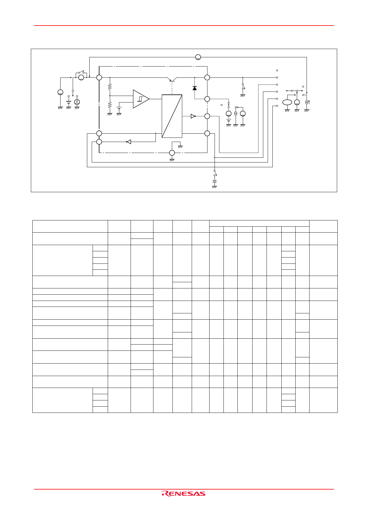
Figure 1 Test Circuit
Switch Matrix
SW
Measuring
Item
Symbol
V1
V2
IF1
IF2
1
2
3
4
5
6
7 Instrument
Circuit current
4V
ICC
—
—
—
1 ON OFF 1 OFF 1
1 Im1
5V
Detection voltage
(VIN negative-going)
VOUT
CS
Ct
RES
RES
VS
(VSL)
Decrease
—
from 5V
2
3
*2
Vm4
—
—
1 ON OFF 1 OFF 4
1 CRT
5
Vm1
6
Difference between input and output
voltage
VDROP
5V
—
–50mA —
1 ON OFF 1 OFF 2
2 Vm2
–80mA
Ct output voltage (high level)
Ct output voltage (low level)
RES output voltage (high level)
RES output voltage (low level)
VOH(Ct)
5V
VOL(Ct)
4V
VOH(RES)
4V
VOL(RES)
5V
—
—
—
1 ON OFF 1 OFF 4
1 Vm4
—
1
—
—
1 ON OFF 1 OFF 5
Vm4
1mA
2
RES output voltage (high level)
RES output voltage (low level)
VOH(RES)
5V
VOL(RES)
4V
—
1
—
—
1 ON OFF 1 OFF 6
Vm4
1mA
2
CS output voltage (high level) *1
VOH(CS)
4V
0V
—
3V
—
1
—
1 ON OFF 1 OFF 3
Vm4
CS output voltage (low level)
VOL(CS)
5V
—
1mA
2
Backup diode leakage current
IR
5V
3V
—
—
1 ON OFF 2 OFF 1
1 Im2
0V
Backup diode forward direction
voltage
VF
0V
—
—
10µA 1 ON OFF 3 ON 1
1 Vm3
Delay time
Response time
VOUT
CS tpd
RES td
RES
2
2
ON
3
—
—
—
—
*3
ON
*4
1 OFF
5
1 CRT
6
Notes: 1. To measure VOH(CS), insert a 1 MΩ resistor between the CS pin and GND.
2. While monitoring each output by Vm4 or CRT, measure the input voltage Vm1 when the output goes from H
to L and L to H. Regarding VSH, raise VIN from 4 V and measure the input voltage Vm1 when the output goes
from H to L and L to H. ∆VS is VSH – VSL.
3. To measure delay time, change VIN from 0 V to 5 V and compare, with respect to each pin, the positive-going
edge observed on a monitor with that of VIN. To measure response time, change VIN from 5 V to 4 V and
compare, with respect to each pin, the negative-going edge observed on a monitor with that of VIN.
4. Set the switch to OFF when measuring response time.
REJ03D0784-0200 Rev.2.00 Jun 15, 2007
Page 4 of 13
Share Link: 