SMH4803 Ver la hoja de datos (PDF) - Summit Microelectronics
Número de pieza
componentes Descripción
Fabricante
SMH4803 Datasheet PDF : 21 Pages
| |||
SMH4803
after another delay PGD. The delays built into the
SMH4803 allow correct sequencing of power to the loads,
e.g. +3V supply must come up before +5V supply. The
delay times are factory programmed. PG2# and PG3#
can be disabled using the ENPGA and ENPGB inputs.
When these inputs are low they override the enable
function produced when the SMH4803 sees a power
good condition.
The PG1#, PG2#, and PG3# outputs have a 12V with-
stand capability so high voltages must not be connected
to these pins. Inexpensive bipolar transistors will boost
the withstand voltage to that of the host supply, see figure
5 for connections.
Output Slew-Rate Control
The SMH4803 provides a current limited Vgate turn-on.
A fast turn-off is performed by internally shorting Vgate to
Vss. Changing the passive components around the
power MOSFET switch will modify the turn-on slew-rate.
Operating at High Voltages
The breakdown voltage of the external active and passive
components limits the maximum operating voltage of the
SMH4803 hot-swap controller. Components that must be
able to withstand the full supply voltage are: the input and
output decoupling capacitors, the protection diode in
series with DrainSense pin, the power MOSFET switch
and capacitor connected between its drain and gate, the
high-voltage transistors connected to the power good
outputs, and the dropper resistor connected to the
controller’s Vdd pin.
Over-Voltage and Under-Voltage Resistors
In the following examples, the three resistors, R1, R2, and
R3, connected to the OV and UV inputs must be capable
of withstanding the maximum supply voltage which can
be several hundred volts. The trip voltage of the UV and
OV inputs is +2.5V relative to Vss. As the input resis-
tances of UV and OV are very high, high value resistors
can be used in the resistive divider. The divider resistors
should be high stability, 1% metal-film resistors to keep
the under-voltage and over-voltage trip points accurate.
Telecom Design Example
A hot-swap telecom application uses a 48V power supply
with a –25% to +50% tolerance, i.e. the 48V supply can
vary from 36V to 72V. The formulae for calculating R1, R2,
and R3 are shown below.
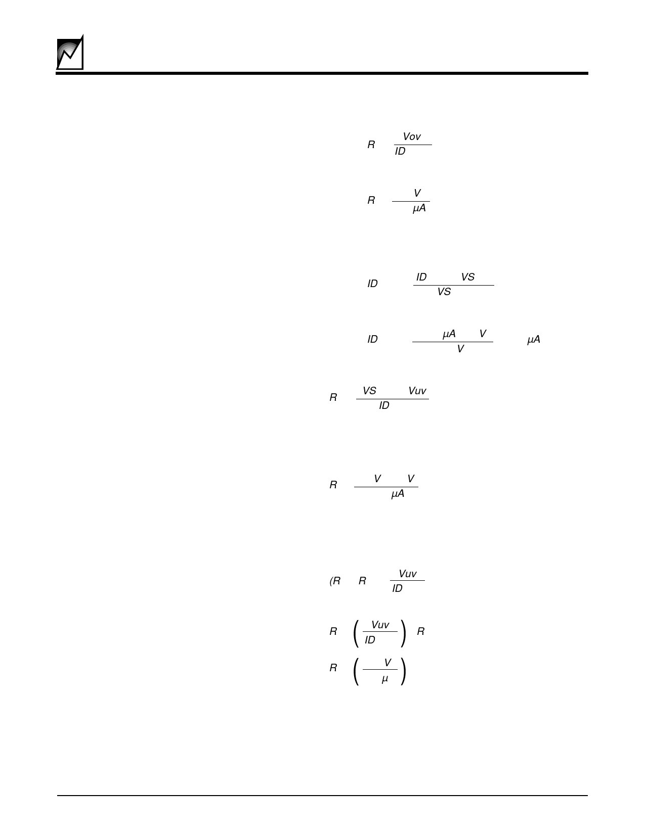
R1 is calculated from:
Vov
R1 = ID max
VOV is the over-voltage trip point, i.e. 2.5V, therefore:
R1 = 2.5V =10kΩ
250 µA
2) The minimum current that flows through the resistive
divider, IDmin, is easily calculated from the ratio of
maximum and minimum supply voltages:
ID min = ID max x VS min
VS max
Therefore:
ID min = 250 µA x 36V = 125 µA
72V
3) The value of R3 is now calculated using IDmin.
R3 = (VS min – Vuv)
ID min
Where Vuv is the under-voltage trip point, also 2.5V,
therefore:
R3 = (36V – 2.5V) = 268kΩ
125 µA
The closest standard 1% resistor value is 267kΩ
4) R2 may be calculated using:
(R1 + R2) = Vuv
ID min
R2 =
Or
R2 =
Vuv
ID min
2.5V
125µA
–R1
–10kΩ = (20kΩ – 10kΩ) = 10kΩ
1) First select the peak current, IDmax, allowed through
the resistive divider, say 250µA. The value of current
is arbitrary; however, if the current is too high, self-
heating in R3 may become a problem (especially in
high voltage systems), and if the current is too low the
value of R3 becomes very large and may be expensive
at 1% tolerance.
SUMMIT MICROELECTRONICS
11
2041 8.4 6/15/00
Share Link: 