M24M01-VLA6 Ver la hoja de datos (PDF) - STMicroelectronics
NГәmero de pieza
componentes DescripciГіn
Fabricante
M24M01-VLA6 Datasheet PDF : 21 Pages
| |||
M24M01
SIGNAL DESCRIPTION
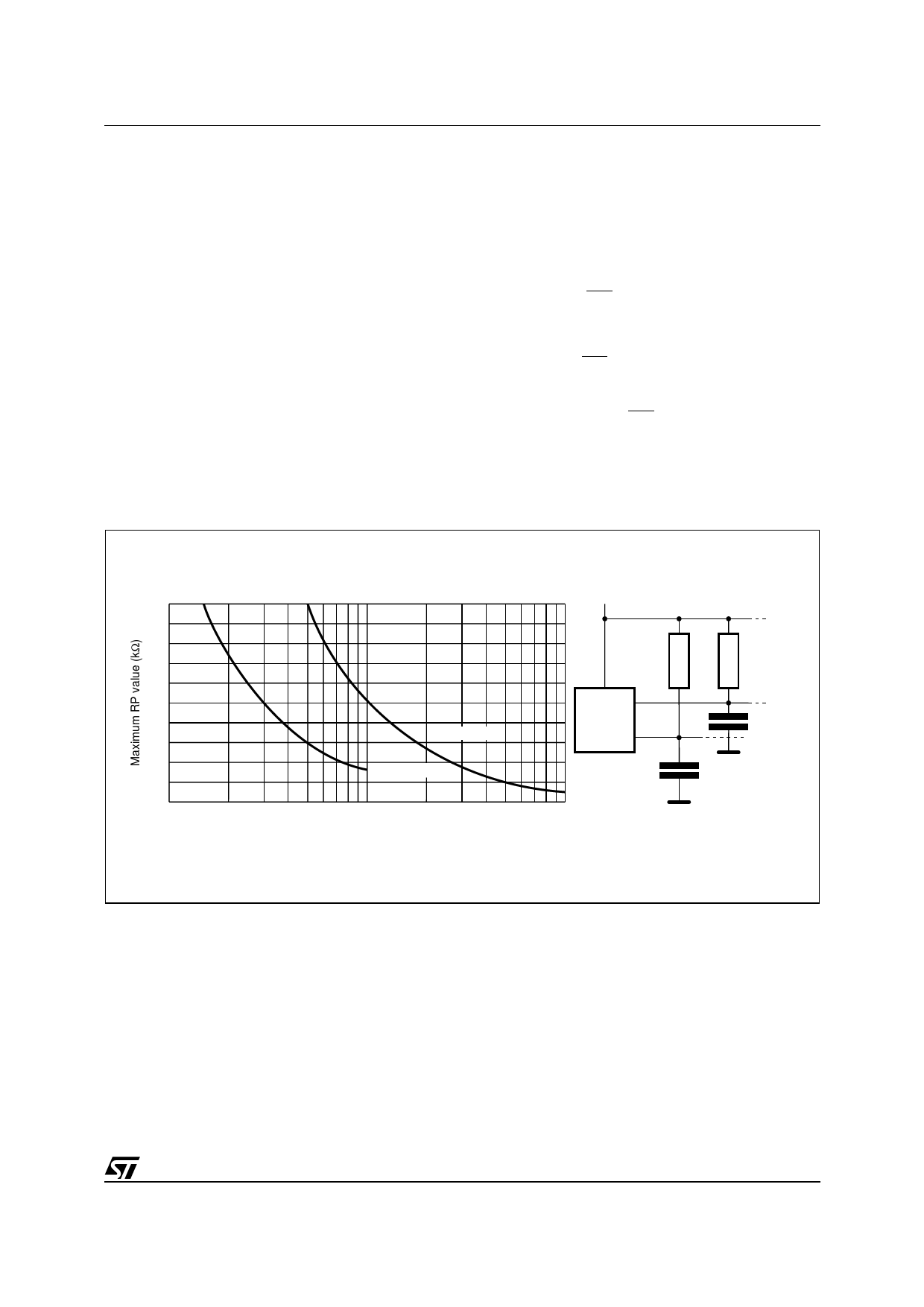
Serial Clock (SCL). This input signal is used to
strobe all data in and out of the device. In applica-
tions where this signal is used by slave devices to
synchronize the bus to a slower clock, the bus
master must have an open drain output, and a
pull-up resistor must be connected from Serial
Clock (SCL) to VCC. (Figure 4 indicates how the
value of the pull-up resistor can be calculated). In
most applications, though, this method of synchro-
nization is not employed, and so the pull-up resis-
tor is not necessary, provided that the bus master
has a push-pull (rather than open drain) output.
Serial Data (SDA). This bi-directional signal is
used to transfer data in or out of the device. It is an
open drain output that may be wire-ORвҖҷed with
other open drain or open collector signals on the
bus. A pull up resistor must be connected from Se-
rial Data (SDA) to VCC. (Figure 4 indicates how the
value of the pull-up resistor can be calculated).
Chip Enable (E1, E2). These input signals are
used to set the value that is to be looked for on bits
b3 and b2 of the 7-bit Device Select Code. These
inputs must be tied to VCC or VSS, to establish the
Device Select Code. When unconnected, the Chip
Enable (E1, E2) signals are internally read as VIL
(see Table 10 and Table 11).
Write Control (WC). This input signal is useful
for protecting the entire contents of the memory
from inadvertent write operations. Write opera-
tions are disabled to the entire memory array when
Write Control (WC) is driven High. When uncon-
nected, the signal is internally read as VIL, and
Write operations are allowed.
When Write Control (WC) is driven High, Device
Select and Address bytes are acknowledged,
Data bytes are not acknowledged.
Figure 4. Maximum RL Value versus Bus Capacitance (CBUS) for an I2C Bus
20
16
12
8
4
0
10
VCC
fc = 100kHz
fc = 400kHz
100
CBUS (pF)
RL
SDA
MASTER
SCL
RL
CBUS
1000
CBUS
AI01665
5/21
Share Link: 