TA7259 Ver la hoja de datos (PDF) - Toshiba
Número de pieza
componentes Descripción
Fabricante
TA7259 Datasheet PDF : 18 Pages
| |||
TA7259P/F/FG
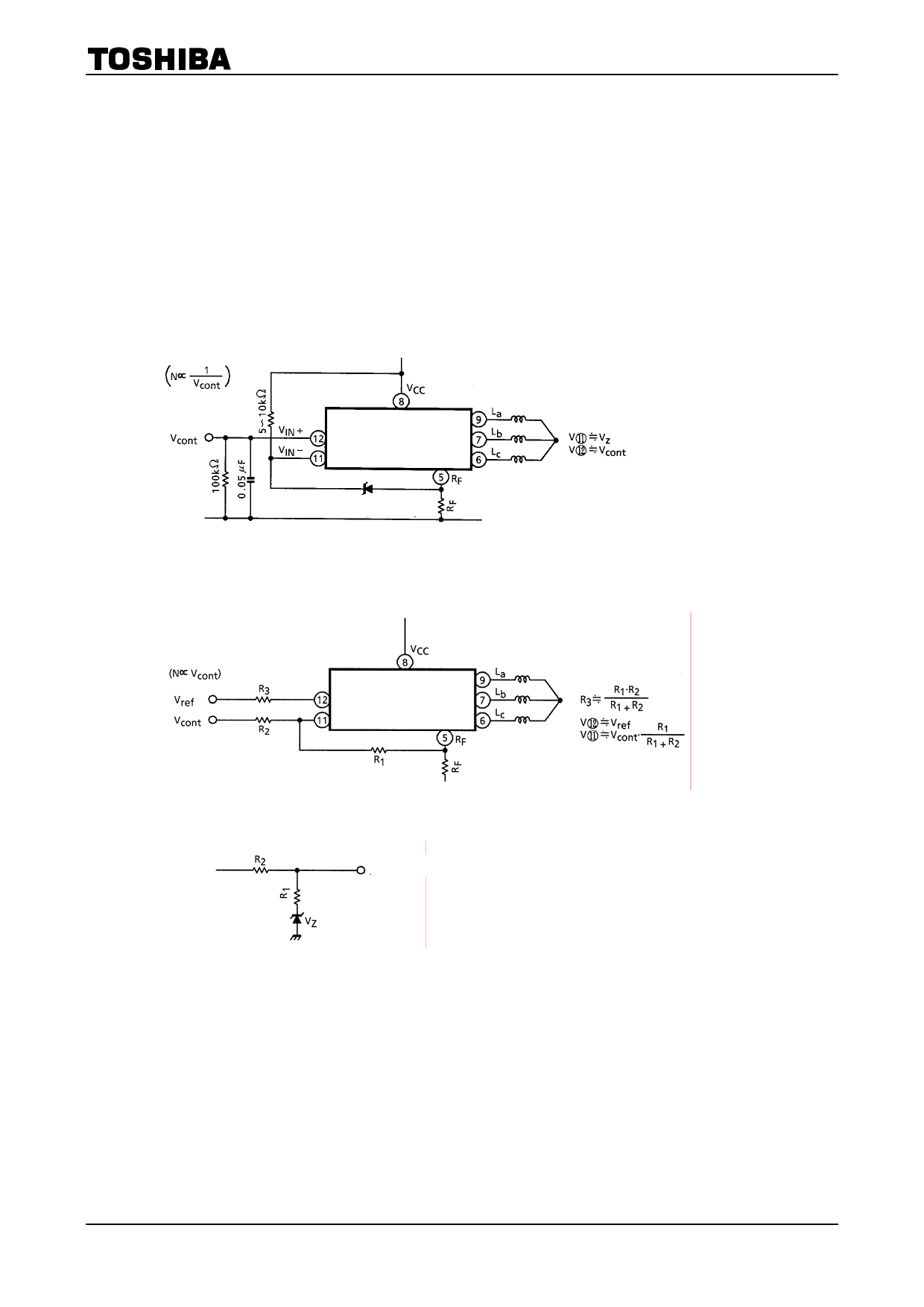
Control signal input
In the initial state of the TA7259P/F/FG, the control voltage is usually input either by an F/V inverter or
such like, where the voltage is in proportion or inverse proportion to the number of rotations, or independently.
Though output (RF pin) gain from the TA7259 control is specified in the table as 15 times, it can be reduced
to improve the characteristics of W/F etc. by applying NF.
An example of the application is shown below.
Whether NF is applied or not, the DC voltage (VIN+ and VIN−) of the control input (VIN+ pin and VIN− pin)
must be within the specified range (2.0 to VCC−2.5V). When the input DC level and F/V conversion output
(control output) cannot interface with the IC input, input DC level shift and attenuator before IC input.
One example is shown in Figure 1−c.
a) Positive input
TA7259P/F/FG
b) Negative input
VZ(5V is recommended)
Figure 1-a
TA7259P/F/FG
Control input
Figure 1-b
Input pin
Figure 1-c
Control output is level shifted with DC content by zenner diode and attenuator, with control signal content by R1
and R2.
5
2006-4-14
Share Link: 